How pcb is made?
July 4, 2022
The primary use of PCBs is to control where the electricity is directed to.The use of a PCB is ubiquitous in today’s society, which has sparked whole fields of electrical engineers and hobbyist tinkerers to create more complex designs.
The PCB manufacturing process can be achieved in a variety of ways and there are a number of variants. Despite the many small variations, the main stages in the PCB manufacturing process are the same.
Printed circuit boards (PCBs) are usually a flat laminated composite made from non-conductive substrate materials with layers of copper circuitry buried internally or on the external surfaces.
They can be as simple as one or two layers of copper, or in high density applications they can have fifty layers or more. The flat composite surface is ideal for supporting the components that are soldered and attached to the PCB, while the copper conductors connect the components to one another electronically.
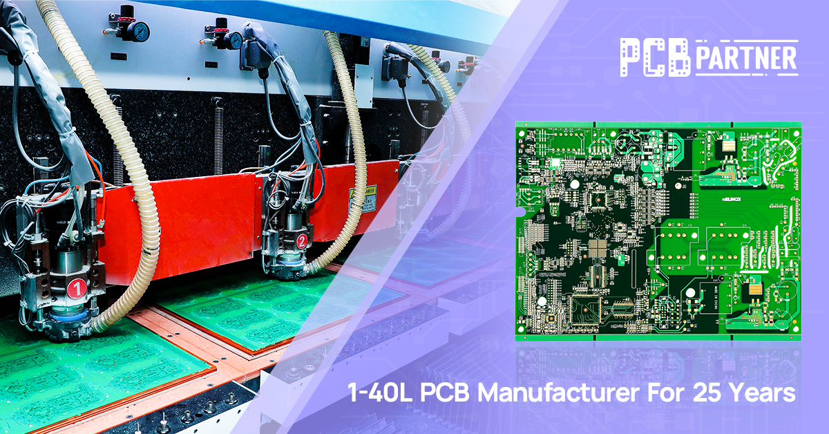
PCB Manufacturing Process
Printed circuit boards are typically made with copper. Depending on the requirements, the copper is plated to a substrate and carved away to expose the design of the board. Since there are multiple layers, they must be lined up and bonded together for a secure fit.
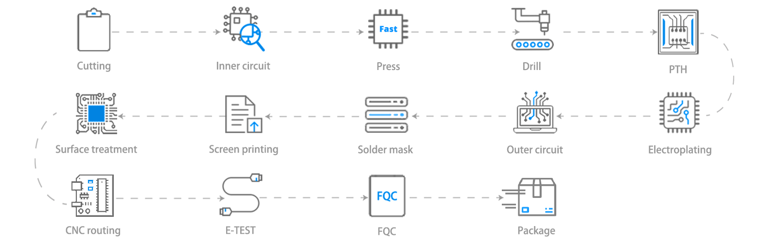
Step 1 – The Design
Before you begin manufacturing the PCB, you need to have a design of the board. These blueprints will be what you base the process off of. The design process is generally completed through computer software. Using a trace width calculator will help with a majority of the details needed for inner and external layers.
Step 2 – Printing the Design
A special printer called a plotted printer is used to print the design of the PCB. It produces a film that shows the details and layers of the board. When printed, there will be two ink colors used on the inside layer of the board:
Clear Ink to show the non-conductive areas; andBlack Ink to show the conductive copper traces and circuits.
The same colors are used for the outer layers, but the meaning of them is reversed.
Step 3 – Creating the Substrate
Now is when the PCB will start to form. The substrate, which is the insulating material (epoxy resin and glass fiber) that holds the components on the structure, begins forming by passing the materials through an oven to be semicured. Copper is pre-bonded to both sides of the layer and then etched away to show the design from the printed films.
Step 4 – Printing the Inner Layers
The design is printed to a laminate, the body of the structure. A photo-sensitive film made from photo-reactive chemicals that will harden when exposed to ultraviolet light (the resist) covers the structure.. This will help align the blueprints and the actual print of the board. Holes are drilled into the PCB to help with the alignment process.
Step 5 – Ultraviolet Light
Once aligned, the resist and laminate go under ultraviolet lights to harden the photoresist. The light reveals the pathways of copper. The black ink from before prevents hardening in areas that will be removed later on. The board is then washed in an alkaline solution to remove the excess photoresist.
Step 6 – Removing Unwanted Copper
Now, it is time to remove any unwanted copper that remained on the board. A chemical solution, similar to the alkaline solution, eats away at the unwanted copper. The hardened photoresist remains intact.
Step 7 – Inspection
The newly-cleaned layers will need to be inspected for alignment. The holes drilled earlier help align the inner and outer layers. An optical punch machine drills a pin through the holes to keep the layers lined up. After the optical punch, another machine will inspect the board to ensure there are no defects. From here on out, you will not be able to correct any missed errors.
Step 8 – Laminating the Layers
Now, you will see the board take shape as the layers are fused together. Metal clamps hold the layers together as the laminating process begins. A prepreg (epoxy resin) layer goes on the alignment basin. Then, a layer of substrate goes over the prepreg followed by a copper foil layer and more prepreg resin. Lastly, there is on more copper layer applied, which is the press plate.
Step 9 – Pressing the Layers
A mechanical press is then used to press the layers together. Pins are punch through the layers to keep them properly aligned and secured, these pins can be removed depending on the technology. If correct, the PCB will go to the laminating press, which applies heat and pressure to the layers. The epoxy melts inside of the prepreg that, along with the pressure, fuses the layers together.
Step 10 – Drilling
Holes are drilled into the layers by a computer-guided drill to expose the substrate and inner panels. Any remaining copper after this step is removed.
Step 11 – Plating
The board is now ready to be plated. A chemical solution fuses all of the layers together. The board is then thoroughly cleaned by another series of chemicals. These chemicals also coat the panel with a thin copper layer, which will seep into the drilled holes.
Step 12 – Outer Layer Imaging
Next, a layer of photoresist, similar to Step 3, is applied to the outside layer before being sent for imaging. Ultraviolet light hardens the photoresist. Any undesired photoresist is removed.
Step 13 – Plating
Just like in Step 11, the panel is plated with a thin copper layer. After this, a thin tin guard is layered to the board. The tin is there to protect the copper of the outside layer from being etched off.
Step 14 – Etching
The same chemical solution from before removes any unwanted copper under the resist layer. The tin guard layer protects the needed copper. This step established the PCB’s connections.
Step 15 – Solder Mask Application
All of the panels should be cleaned before the solder mask is applied. An epoxy is applied with the solder mask film. The solder mask applies the green color you typically see on a PCB. Any unwanted solder mask is removed with ultraviolet light, while the wanted solder mask is baked on to the board.
Step 16 – Silkscreening
Silkscreening is a vital step since this process is what prints critical information onto the board. Once applied, the PCB passes through one last coating and curing process.
Step 17 – Surface Finish
The PCB is plated with either a solderable finish, depending on the requirements, which will increase the quality/bond of the solder.
Step 18 – Testing
Unassembled circuit boards are subjected to a bare board test where each circuit connection is verified as correct on the finished circuit board. In high volume circuit board production, a bed of nails tester or fixture is used to make contact with the copper lands or holes on one or both sides of the board to facilitate testing. Computers are used to control the electrical testing unit to send a small current through each contact point on the bed of nails and verify that such current can be detected on the appropriate contact points.
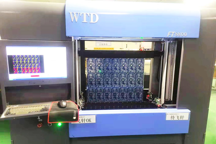
For small to medium volume production runs, a flying probe tester is used to check electrical contacts. These flying probes employ moving heads to make contact with the copper lands and holes to validate the electrical connectivity of the board being tested.
The PCB manufacturing process is an essential element of the electronics production lifecycle. PCB manufacturing employs many new areas of technology and this has enabled significant improvements to be made both in the reduction of sizes of components and tracks used, and in the reliability of the boards.
Get your pcb online quote at Qinji Group’s PCBPartner.com, where hundreds of new customers come to us every day, they stay with us for all their future PCB needs, and of course they can get lower prices Price, higher quality PCB, and better service.