How To Design A PCB Board
July 13, 2022
As a PCB engineer, you must master how to quickly design a successful and excellent PCB circuit board, so that you are on the road to achieving a fast, reliable, professional-quality PCB.
PCB prototype boards have developed from single-sided to double-sided, multi-layer and rigid-flex pcb, and still, maintain their development trends.
Due to the continuous development in the direction of high precision, high density, and high reliability, continuous reduction in size, cost reduction, and performance improvement, printed circuit boards still maintain a strong vitality in developing electronic equipment in the future. So, how to design a PCB board?
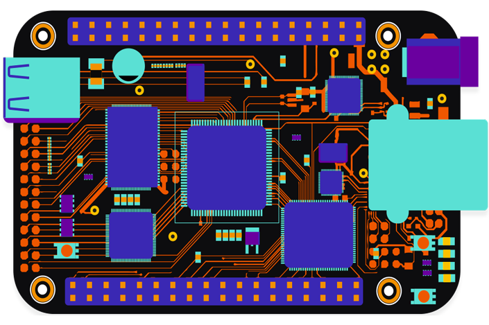
Including the preparation of component library and schematic diagram. Before designing the PCB, first, prepare the schematic SCH component library and the PCB component package library.
The PCB component package library is best established by the engineer based on the standard size data of the selected device. The PCB component package library has high requirements, which directly affects the PCB installation.
The schematic diagram SCH component library requirements are relatively loose, but attention to defining the pin attributes and the corresponding relationship with the PCB component package library.
2. PCB structure design
According to the determined circuit board size and various mechanical positioning, draw the PCB board frame in the PCB design environment, and place the required connectors, buttons/switches, screw holes, assembly holes, etc. according to the positioning requirements.
3. PCB layout design
Layout design is to place devices in the PCB frame according to the design requirements. Generate a netlist in the schematic tool, and then import the netlist into the PCB software.
After the network table is imported successfully, it will exist in the software background. All devices can be called out through the Placement operation, and there are flying wires between the pins to indicate the connection.
At this time, the layout design of the device can be carried out. PCB Layout design is the first important process in the entire PCB design process. The more complex the PCB board, the more the quality of the layout can directly affect the difficulty of the later wiring.
4. PCB wiring design
PCB wiring design is the most work-intensive process in the entire PCB design, which directly affects the performance of the PCB board. In the PCB design process, there are generally three realms of wiring. The first is routing,
which is the most basic entry requirement for PCB design; the second is the satisfaction of electrical performance, which is the standard for measuring whether a PCB board is qualified.
After the circuit is laid out, carefully adjust the wiring to make it the best The electrical performance is excellent; once again, the wiring is neat and beautiful, and the wiring is disordered.
Even if the electrical performance is passed, it will bring great inconvenience to the later board modification optimization, testing, and maintenance.
5. Wiring optimization and silk screen placement
“PCB design is not the best, only better”, and “PCB design is a flawed art”, this is mainly because PCB design needs to meet the design requirements of all aspects of hardware, and individual requirements may conflict, fish and You can’t have both.
6. Network DRC inspection and structure inspection
Quality control is an important part of the PCB design process. General quality control methods include design self-inspection, design mutual inspection, expert review meetings, special inspections, etc.
A schematic diagram and a structural element diagram are the most basic design requirements. Network DRC inspection and structural inspection are to confirm that the PCB design satisfies the two input conditions of the schematic netlist and structural element diagram respectively.
7. PCB board
Before the PCB is formally processed and made, the circuit board designer needs to communicate with the EQ of the PCB supplier and answer the manufacturer’s confirmation questions about the PCB board processing.
This includes but is not limited to the selection of PCB sheet models, the adjustment of line width and spacing of circuit layers, the adjustment of impedance control, the adjustment of PCB stacking thickness, the surface treatment process, the control of aperture tolerance, and delivery standards, etc.
A low-cost PCB bare board does not mean that it will be of poor quality. Low-cost printed circuit board manufacturer in China, the most competitive, cheapest, and affordable PCB manufacturer with zero defects.
PCBpartner is such a company that has mastered all PCB manufacturing technology, zero-defect very competitive and affordable price. In addition to better product quality, the company also offers a lot of premium services.
Whether your needs are PCB prototypes or small and medium-sized rapid production, PCBpartner can do all the work at the cheapest price and with the best service without compromising on quality.


