Sorry, no sales person is available right now to take your call. Pls leave a message and we will reply to you via email as soon as possible.


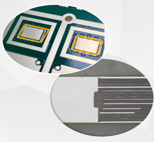
8-Layer Hybrid Embedded Metal Base PCB | Kinji RO4350B Thermal Solution
Kinji 8-layer hybrid embedded metal base PCB with RO4350B delivers extreme heat dissipation (tens of times > FR-4) and ≤15μm flatness. Ideal for 5G RF PAs/AAU modules – lowers junction temp by 18°C, boosts SMT yield to 99.8%. Sample lead time 10+ days.
2026-04-17
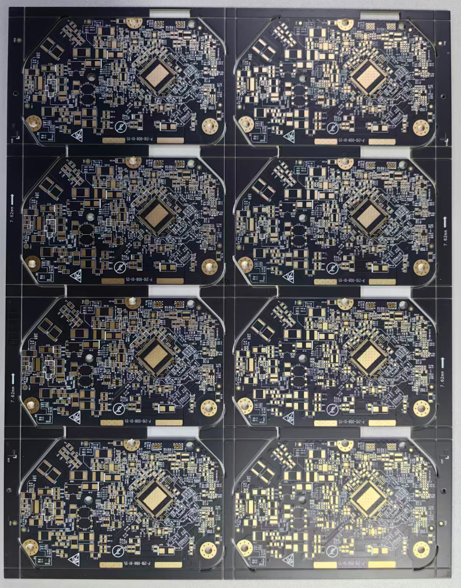
6-Layer Black Oil PCB: The Smart Choice for Automotive Wireless Charging Modules
Kinji Cloud Board introduces its 6-layer black oil PCB (7mil IC, 4mil black oil bridge) – a precision-engineered solution designed specifically for automotive wireless charging modules, delivering reliability, efficiency, and signal integrity under demanding vehicle conditions.
2026-04-17
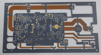
Qinji PCB 6-Layer HDI Rigid-Flex Board: High Density & Reliability
As smart devices continue to pursue slimmer profiles and higher performance, traditional PCBs can no longer meet the demands of complex application scenarios. Qinji’s newly launched 6-layer HDI rigid-flex PCB, with its innovative structure and premium manufacturing process, redefines the possibilities of high-density interconnection.
2026-03-18
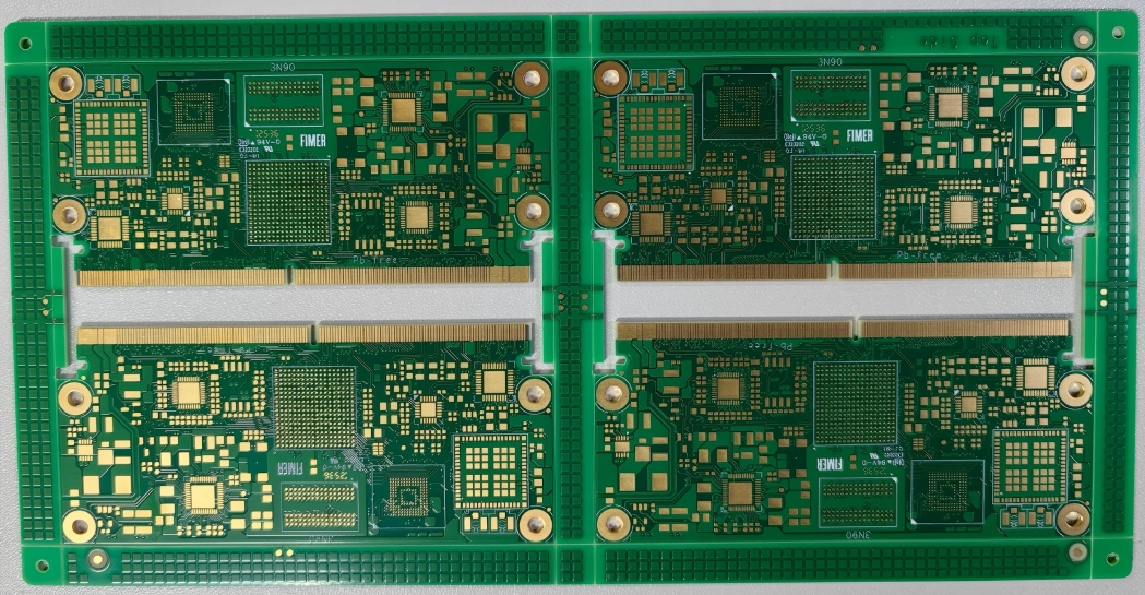
Qinji 10-Layer 1+1 HDI Board for New Energy Power Electronics
In the field of new energy power electronics (PV / energy storage / EV charging piles), PCBs are subject to extremely high requirements for precision, reliability and integration density. The 10-layer 1+1 HDI board launched by Qinji PCB Cloud is a high-performance solution designed to meet these stringent demands.
2026-03-18
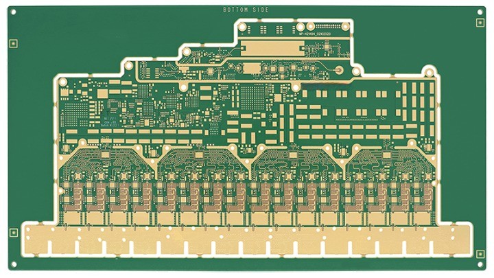
High-Frequency PCB vs High-Speed PCB: Stop Confusing Them!
They seem similar: both are high-end PCBs that require impedance control and signal quality assurance. They are often used together: one board can carry both RF and high-speed digital signals. Industry habit: People commonly say "high-frequency and high-speed boards", so they gradually become regarded as a single concept. But in professional design and manufacturing, they follow completely differe
2026-02-25
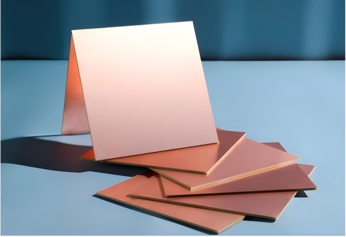
PCB Copper Thickness Conversion Table (oz–μm–mil) & 1oz Copper Thickness Explanation
In PCB production communication and specification sheets, we often hear "1oz copper thickness" and default that it corresponds to approximately 35 microns (μm). This seemingly regular value is not arbitrarily set, but a result of precise physical definitions, unit conversions, and industry practice conventions. The logic behind it is clearly explained from three aspects: definition, conversion, an
2026-02-25

Contact Us