


Sorry, no sales person is available right now to take your call. Pls leave a message and we will reply to you via email as soon as possible.
The PCB difference between pads (Pad) and vias (Via)
2025-04-01
Solder pads are metal contact points on a PCB (Printed Circuit Board) used for soldering components, and they are also referred to simply as pads. They are formed through a copper coating process and are typically located on the surface and inner layers of the PCB.
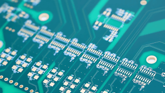
PCB Solder Pads
Types of Solder Pads
Depending on their purpose and manufacturing technology, solder pads can be classified into the following types:
- Pin Pads: Pin pads are metal contact points used to solder pin components onto the PCB. They usually consist of circular or elliptical metal rings, into which the pins can be directly inserted for soldering.
- Surface Mount Pads: Surface mount pads are metal contacts for electronic components that are soldered onto the surface of the PCB using SMT (Surface Mount Technology). They are typically flat metal pads used to connect the solder pins of SMT components.
- Through-Hole Pads: Through-hole pads are metal contact points located on both the surface and inner layers of the PCB, commonly used for soldering pin components or connecting internal circuits. They consist of a metal ring and a conductive hole.
Functions of Specialized PCB Pads
- Feathered Pads: The fixing holes require non-metallization and adopt a plum blossom hole design, which ensures that the screws remain grounded regardless of stress changes. Fixing mounting holes are often used as plum blossom pads for the GND network of mounting holes and sometimes serve as shielding for the PCB enclosure.
- Cross-Pattern Pads: Cross-shaped pads are mainly used to reduce the heat dissipated by the pads during the soldering process, preventing PCB delamination or solder failure.
- Teardrop Pads: Teardrops refer to the transitional connections between pads and wires or between wires and holes. Implementing teardrops can effectively prevent wires from breaking off at the hole pads or wire contact points, while also enhancing the aesthetic appearance of the PCB.
Differences Between Pads and Vias
- Concept
Solder pads are reserved positions on the PCB for soldering chips or components. On the PCB, the pins of components are soldered to the pads, thereby achieving both electrical and physical connections between the components and the circuit board. Therefore, pads are required on every layer of the PCB.
Vias are small holes on the PCB surface that provide electrical connections to another layer (in the case of a double-sided board) or multiple layers (in the case of a multi-layer board). Through vias, connections between different layers can communicate with each other, making PCB routing more flexible.
- Function
Solder pads connect components, achieving both physical and electrical connections between the components and the circuit board.
Vias, on the other hand, connect different parts of the circuit between layers, ensuring the normal operation of the circuit.
- Shape and Design
Solder pads are usually circular or square, with their size and shape depending on the requirements of the components. In pad design, it is important to ensure that the pad size meets the soldering requirements of the top components and to consider the spacing between components to avoid short circuits due to excessive proximity.
Vias are created through electrolytic copper plating. In design, the position and diameter of the vias need to be considered. For multi-layer PCBs, the number and distribution of vias also need to be taken into account to ensure power efficiency and signal transmission stability.
- Processing Method
Solder pads are typically made through electroless copper plating, followed by electroplating of the outer layer of the pad to ensure its corrosion resistance and conductivity.
Vias are created by drilling holes on the board surface and then applying electroless copper plating.
Although there are different types of PCB solder pads, their functions are consistent. Firstly, they achieve electrical connections for electronic components in the circuit; secondly, they enable external electronic components to be better connected to the PCB, serving as a means to prevent detachment.
Previous Article: How to select high-frequency PCB and high-speed PCB materials
Next Article: The PCB difference between pads (Pad) and vias (Via)
trending news
Contact Us