

Sorry, no sales person is available right now to take your call. Pls leave a message and we will reply to you via email as soon as possible.
Introduction of common ceramic surface metallization technology for electronic packaging ceramic substrates
2024-10-29
There is an increasing demand for ceramic substrate surface metallization technology in the field of electronic packaging to meet the requirements of high current, high voltage powered integrated circuit components and equipment miniaturization. The following is a detailed introduction to this technology.
The importance of surface metallization of ceramic substrates
After sintering, the surface of the ceramic substrate needs to be metallized to complete the production of surface graphics and achieve electrical connection performance. The wetting ability of metal on ceramic surface at high temperature determines the binding force between metal and ceramic, and good binding force is an important guarantee for the stability of packaging performance.
ectronic packaging applications such as high-density DC/DC converters, power amplifiers, RF cirCommon metallization methods for ceramic surfaces
| Comparison item | LTCC | HTCC | TFC | DBC | DBA | DPC |
| Thermal conductivity/(W/(m·K)) | 2~3( Al₂O₃) | 16~ 24( Al₂O₃) | 16~ 24( Al₂O₃) | 16~ 24( Al₂O₃) | 16~ 24( Al₂O₃) | 16~ 24( Al₂O₃) |
| 170~235( AIN) | 170~235( AIN) | 170~235( AIN) | 170~235( AIN) | |||
| Process temperature/℃ | 850~1000 | 1300~1600 | 700~800 | 1020~1100 | 1020~1100 | 250~350 |
| Graphic production method | Screen printing | Screen printing | Screen printing | Hot press bonding | Hot press bonding | Film + electroplating |
| Surface metal material | Silver, copper, gold, etc | Tungsten, molybdenum, manganese, etc | Silver, copper, gold, etc | Copper | Aluminum | Copper |
| Through hole filling mode | Screen printing | Screen printing | Screen printing | Electroplating, electroless plating | Electroplating, electroless plating, etc | Electroplating, electroless plating, etc |
| Scope of application | Communication, positioning system, digital circuit, LED, etc | Communication, positioning system, digital circuit, LED, etc | Satellite communication equipment, aerospace electronic equipment, LED, etc | LED, ICBT, IPG and other large power electronic components | Insulating carriers, especially high-power electronic circuits | LED, ICBT, IPG and other large power electronic components |
| Advantage | The technology is mature and the cost is low. | The technology is mature and the thermal conductivity is high. | The technology is mature, the process is simple and the cost is low. | Accurate alignment, no difference in sintering shrinkage | Accurate alignment, no difference in sintering shrinkage | Accurate alignment, no difference in sintering shrinkage, can produce 10-50um lines |
| Disadvantage | Poor alignment accuracy, rough surface of the line | Poor alignment accuracy, rough line surface, high cost | Rough surface, inaccurate alignment | Copper coating resolution is too large, need processing | Copper coating resolution is too large, need processing | The copper layer is only 3-5um and needs to be thickened by electroplating |
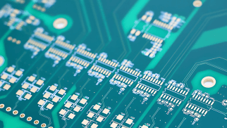
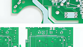
Application of ceramic metallized substrate
Ceramic metallized substrates are primarily used in elcuits, and high-current switches. These ceramic metallized substrates take advantage of the electrical conductivity of metals as well as the good thermal conductivity, mechanical strength properties and low electrical conductivity of ceramics.
Technical requirements for surface metallization of ceramic substrates
Excellent sealing, small square resistance and resistivity of the metal conductive layer, strong adhesion with the ceramic substrate and high thermal conductivity of the ceramic substrate after metallization are the main technical requirements for the surface metallization of the ceramic substrate.
In summary, the surface metallization technology of electronic packaging ceramic substrate has a variety of methods, each of which has its unique advantages and scope of application. With the continuous development of technology, these metallization technologies will play an increasingly important role in the field of electronic packaging.
*Disclaimer: This article is from the Internet, if there is any dispute, pleasecontact customer service.
trending news
Contact Us