

Sorry, no sales person is available right now to take your call. Pls leave a message and we will reply to you via email as soon as possible.
Understanding Common Stack-Up Designs in HDI Boards
2025-04-16
In today's electronics manufacturing industry, High-Density Interconnect (HDI) technology is a critical driver for achieving miniaturization and high performance in electronic products. The key advantage of HDI lies in its precision stack-up design, which not only enhances space utilization efficiency but also improves electrical performance and signal integrity. By optimizing circuit layouts and reducing signal delays, HDI provides a robust foundation for innovation, enabling smaller, faster, and more powerful devices. Furthermore, this technology has propelled advancements across industries such as mobile devices, computing, and automotive electronics.
Optimized Interconnectivity and Space Efficiency
HDI stack-up designs enable multilayer interconnections through precisely controlled blind and buried vias, which have diameters significantly smaller than traditional PCB through-holes. These microvias reduce the overall board size while increasing wiring density, allowing more components to be integrated into compact spaces. This is essential for modern electronics that prioritize high performance and miniaturization, offering unprecedented opportunities for innovation.
Enhanced Signal Integrity
HDI stack-up designs optimize signal transmission paths by shortening distances and minimizing unnecessary bends. This reduces signal delay and loss, which is critical for high-speed devices handling large data volumes. Improved signal integrity ensures faster and more accurate data processing, enhancing overall device reliability. Such optimizations are vital in today’s high-tech landscape, where speed and precision are paramount.
Manufacturing Challenges
Producing HDI boards requires advanced laser drilling and precision etching equipment to achieve high-accuracy blind/buried vias and layer alignment. Rigorous testing and validation of materials and processes are also essential to ensure reliability.
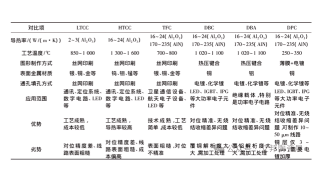
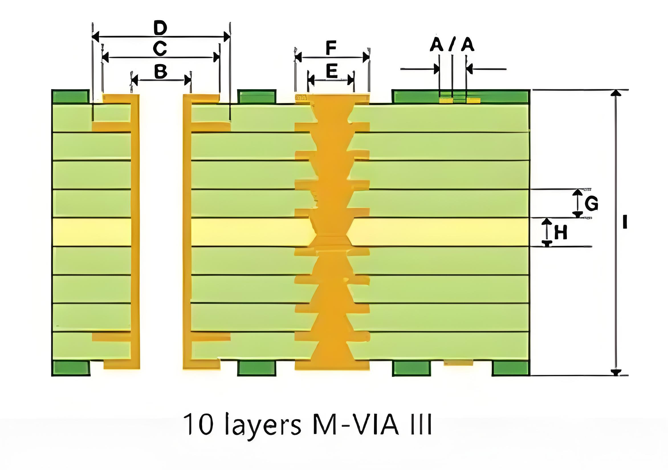
Common HDI Stack-Up Types
To meet diverse engineering needs, several HDI stack-up configurations exist:
1. 1+N+1 Structure
- Terminology: The "1" refers to blind vias (1-step microvias) on each outer layer, while "N" denotes internal signal layers (e.g., 1-4-1 for a 6-layer board).
- Process: A core (CCL) is laminated into a 4-layer board, then further laminated to form 6 layers. This is a mainstream "2-lamination" process.
- Typical Application: Cost-effective designs requiring moderate density.
2. 2+N+2 Structure
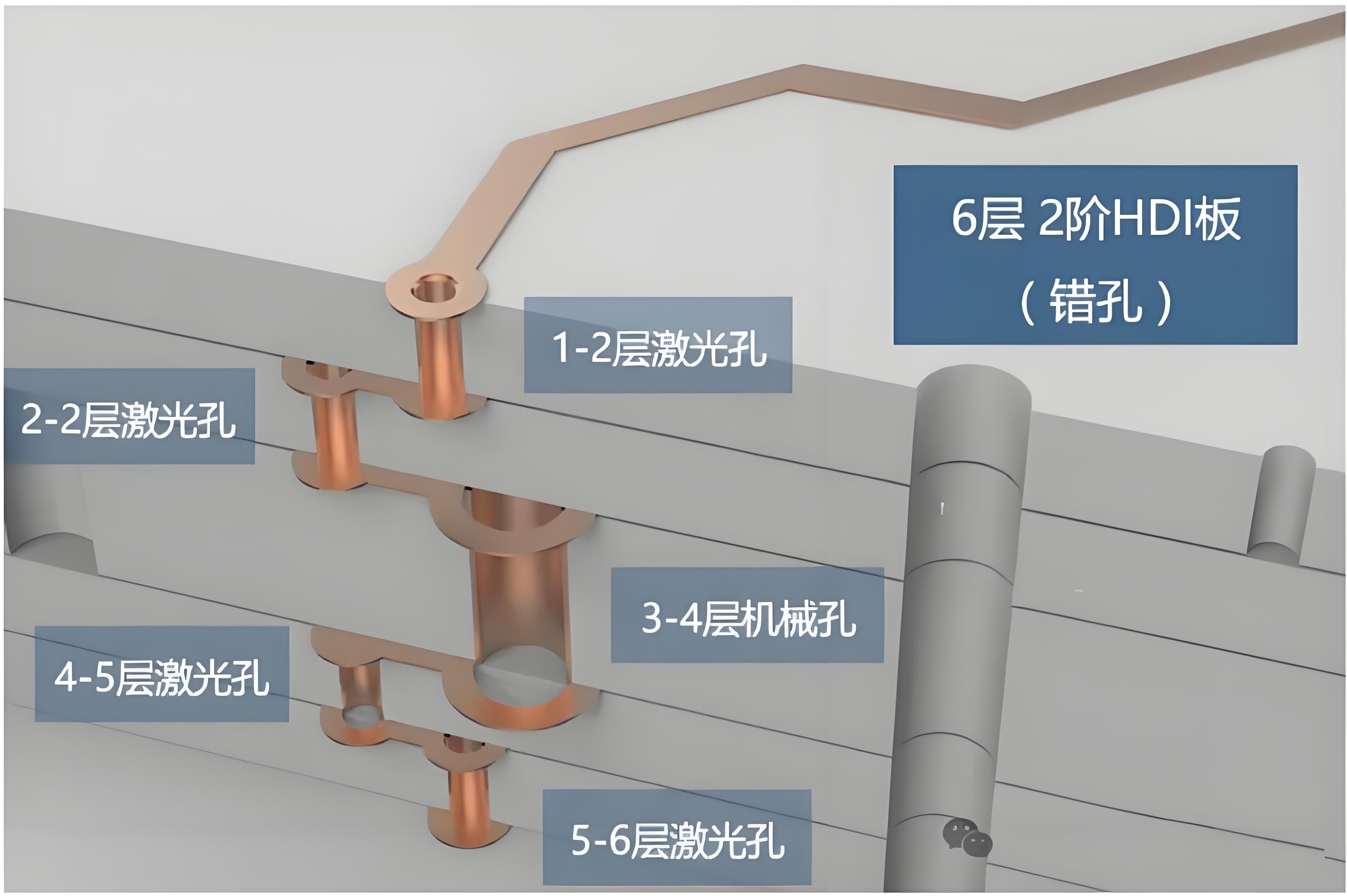
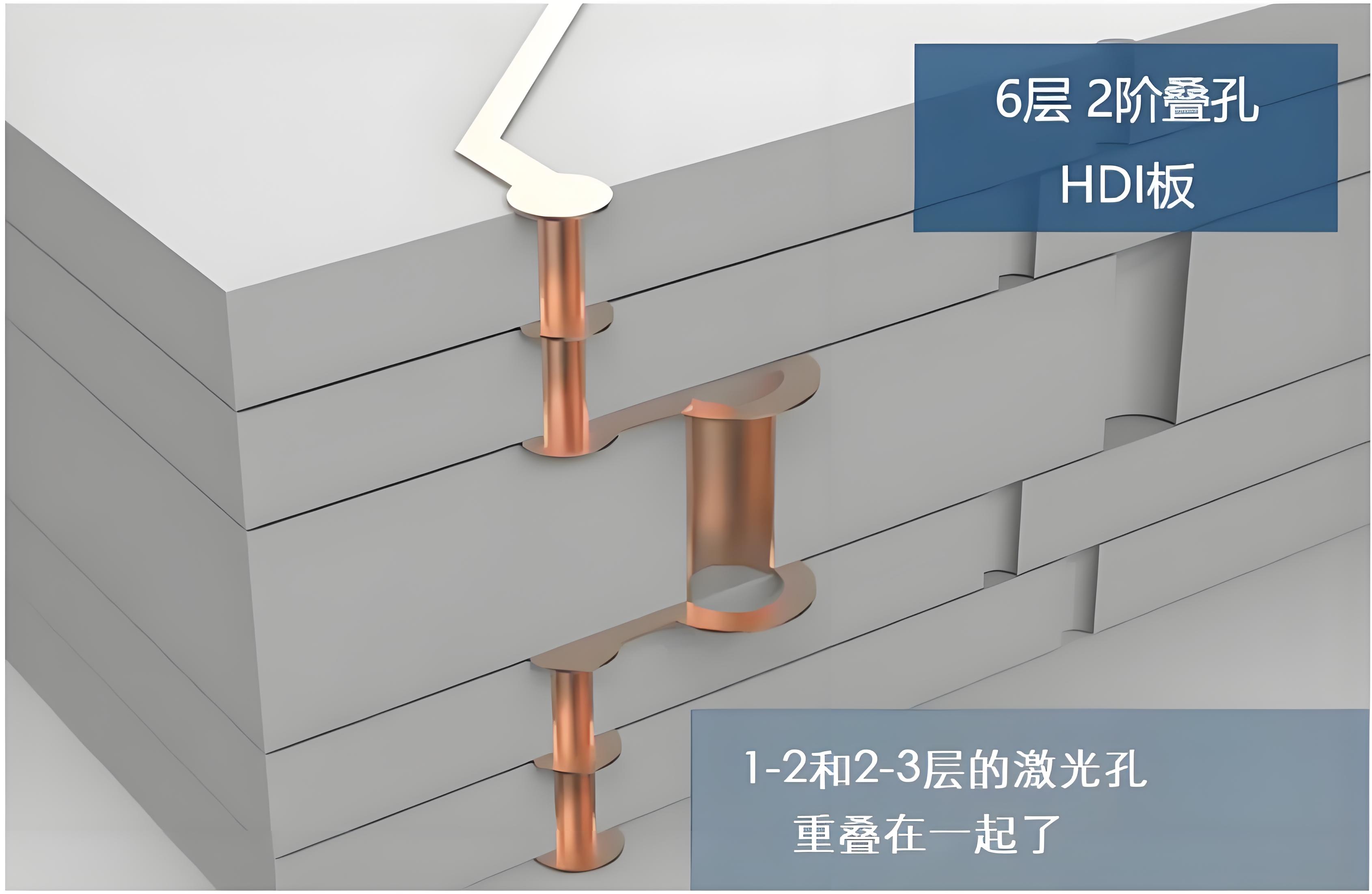
- Terminology: Two layers of blind vias (2-step) on each side, with internal layers (N).
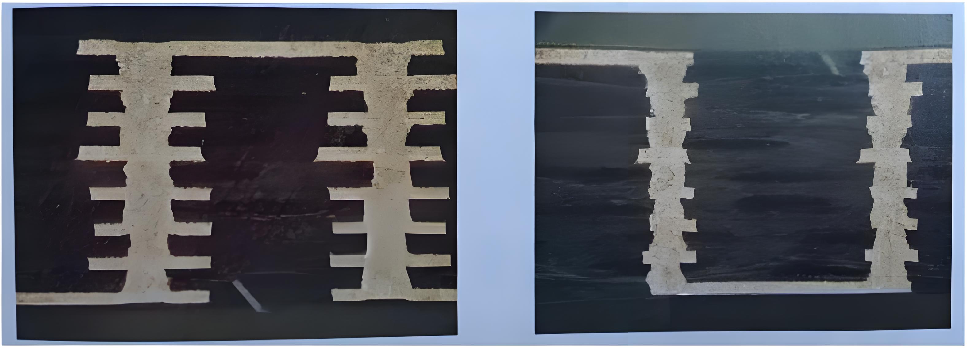
- Design Variations:Staggered Vias: Lower cost and high reliability, with offset via stacking.Stacked Vias: Requires filling prior vias with conductive/resin materials for sequential drilling. This increases complexity but supports higher density.
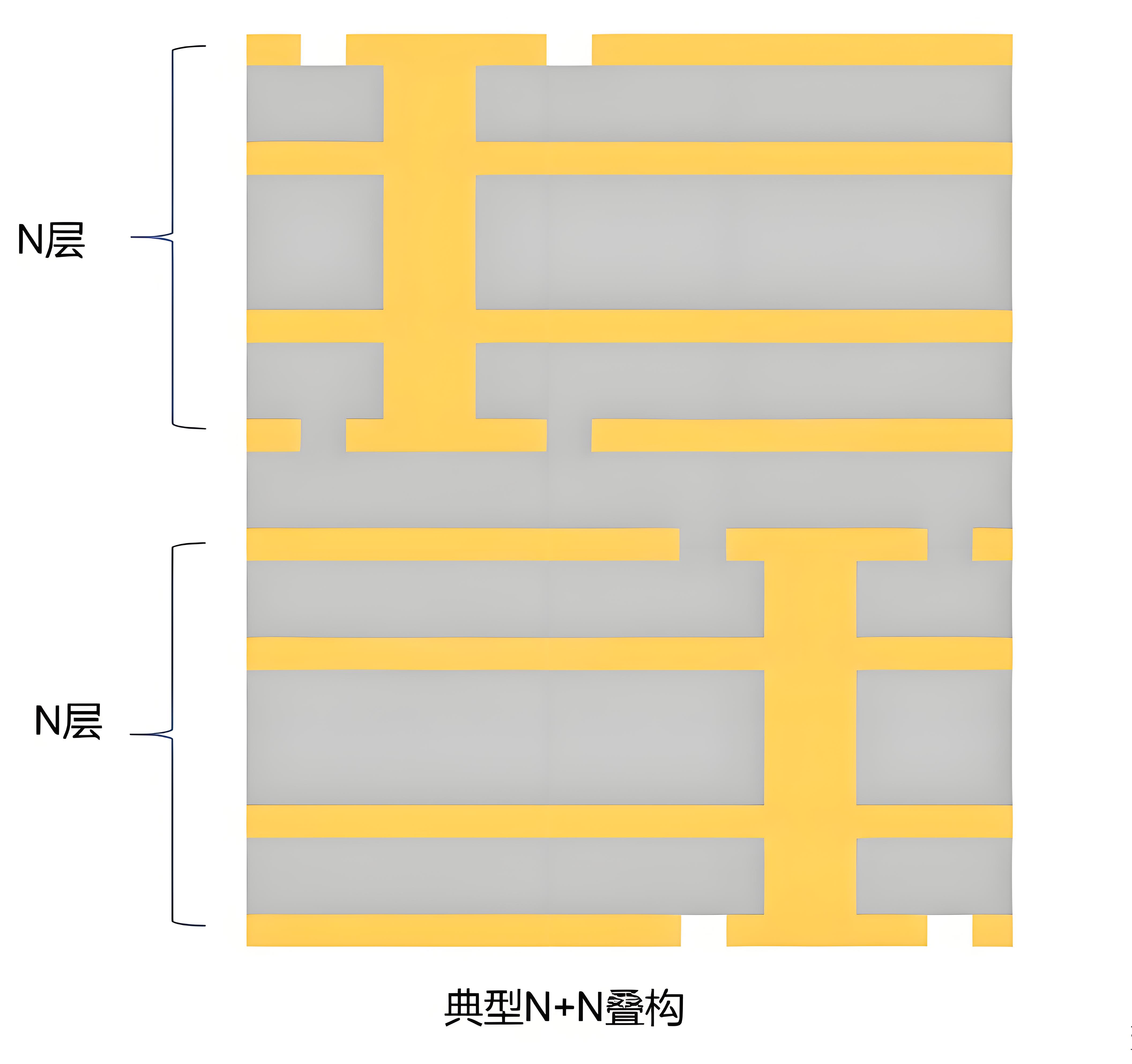
3. N+N Structure
- Terminology: A non-HDI configuration with no blind vias but strict alignment requirements.
- Challenge: Despite lacking microvias, its production difficulty rivals HDI due to precision demands.
4. AnyLayer Interconnect (ELIC)
- Terminology: Enables connections between any layers via stacked or staggered microvias.
- Technology: Relies on Modified Semi-Additive Process (MSAP) for ultra-fine lines and precision.
- Challenge: Demands exceptional layer alignment and advanced laser/etching capabilities.
Conclusion
Despite its challenges, HDI stack-up design has become indispensable in high-end electronics. From smartphones and wearables to advanced computing and communication systems, HDI enables smaller, faster, and more reliable devices. As technology evolves and consumer demands grow, HDI will continue to drive innovation in electronics manufacturing. Future breakthroughs in HDI-based products promise to reshape industries and redefine technological possibilities.
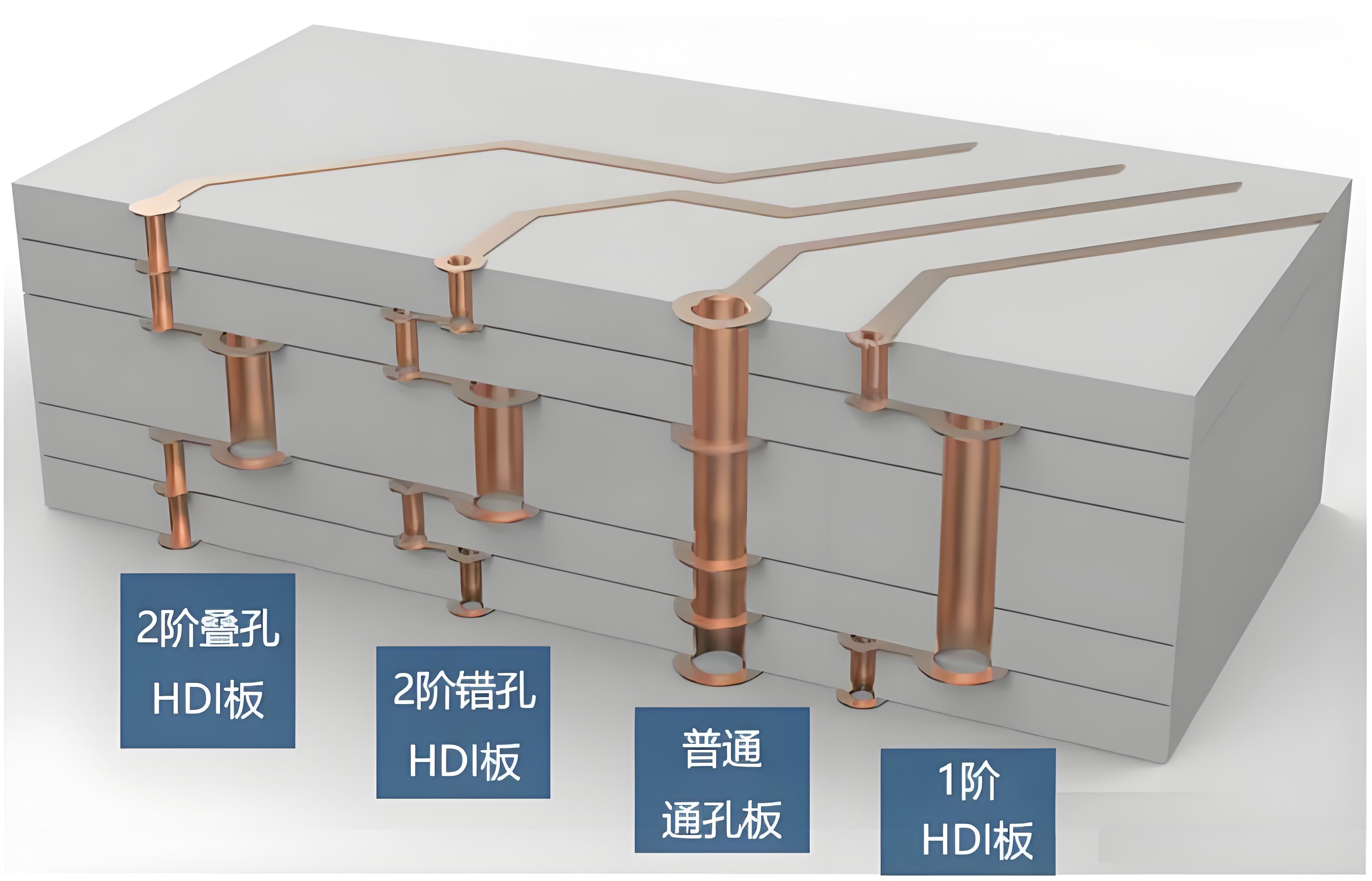
Visual Summary of Key Stack-Up Designs
(Note: Diagrams mentioned in the original text would illustrate the layer arrangements and via structures for each configuration.)
- 1+N+1 Stack-Up:Surface layers with 1-step blind vias connected to internal layers.
- 2+N+2 Stack-Up:Staggered vs. stacked vias, highlighting material filling and lamination steps.
- AnyLayer (ELIC):Cross-sectional view of stacked microvias enabling interlayer connections.
Previous Article: The PCB difference between pads (Pad) and vias (Via)
Next Article: Understanding Common Stack-Up Designs in HDI Boards
trending news
Contact Us