
Sorry, no sales person is available right now to take your call. Pls leave a message and we will reply to you via email as soon as possible.

PRODUCT DETAILS
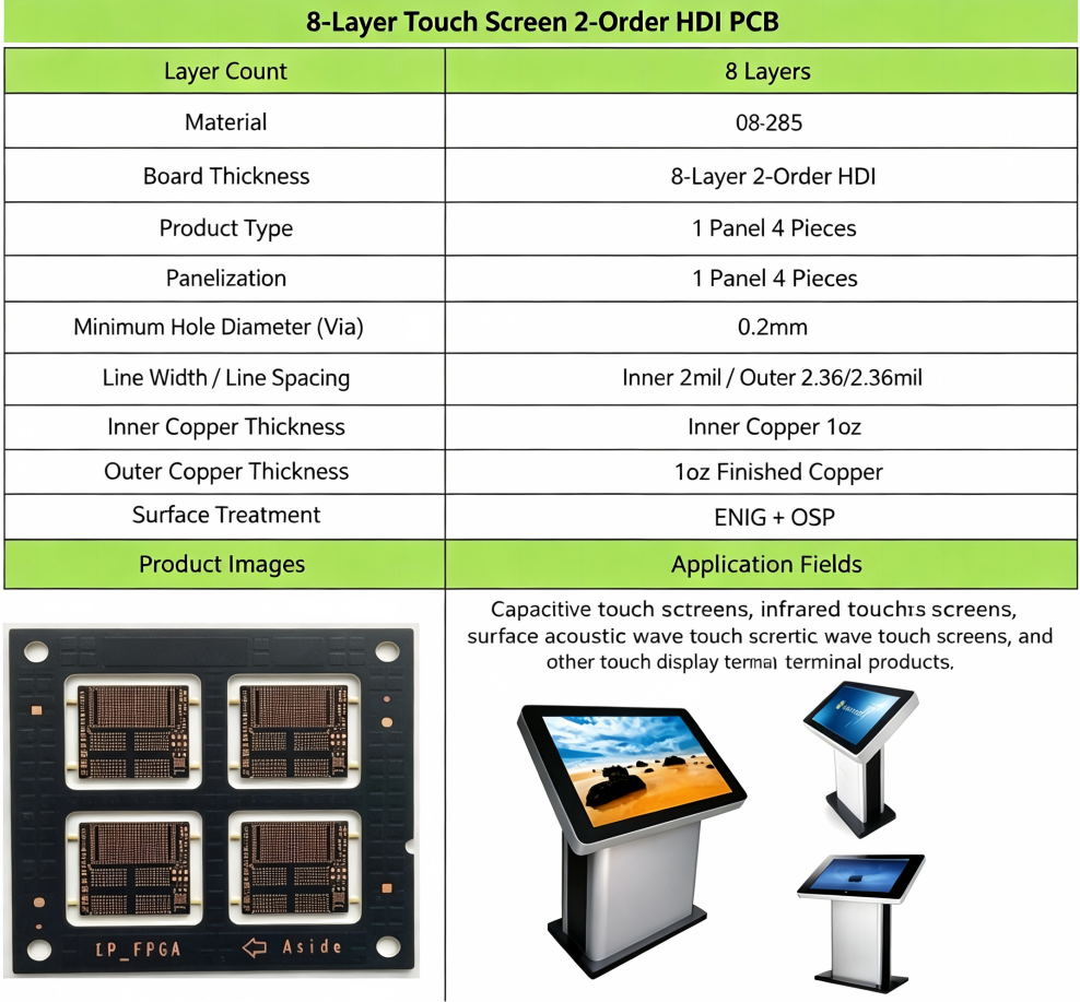
Process & Performance Analysis
Advantages of 2-Level HDI Technology
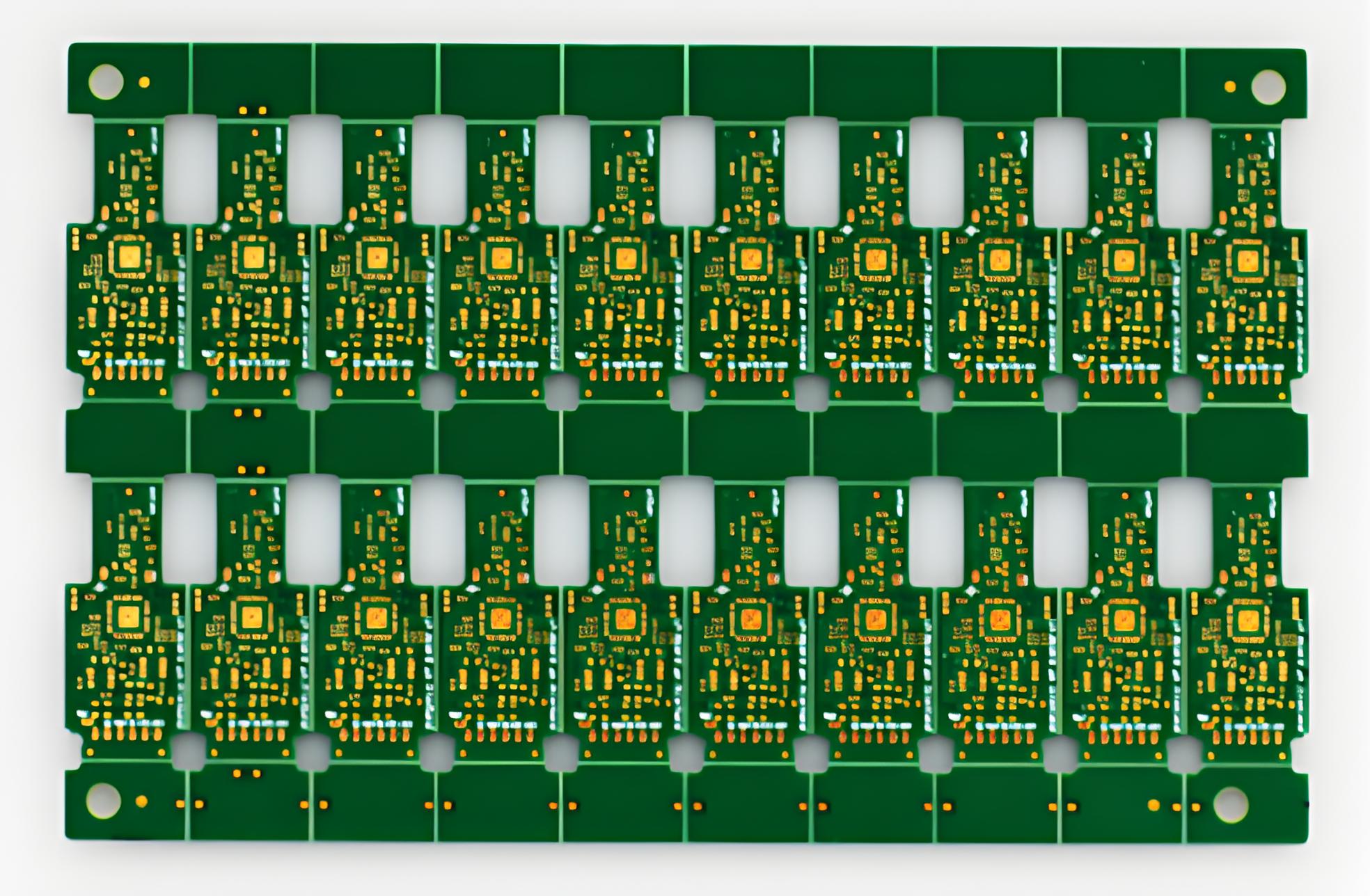
The 2-level blind & buried HDI structure enables dense routing and microvia interconnection, perfectly matching the high-density pin layout of FPGA chips. With an ultra-thin board thickness of 0.8 mm, it balances routing density and board rigidity, making it a mainstream high-end manufacturing process for touch industrial control mainboards.
Line Width & Aperture Capability
It supports a minimum line width & spacing of 2 mil on inner layers and a 0.2 mm microvia hole size, delivering ultra-high circuit integration to meet high-density routing requirements for touch signal acquisition, signal transmission and FPGA logic operation.
Copper Thickness & Surface Finish
0.5 oz thin copper for inner layers suits fine-line etching of inner circuits; 1 oz copper on outer layers ensures current-carrying capacity for high-current loops.
ENEPIG is applied on precision BGA pads to improve solderability and anti-oxidation performance. OSP is adopted for general circuits to control manufacturing cost, achieving a good balance between performance and cost-effectiveness.
Properties of EM-285 Substrate
This material features stable heat resistance and dielectric properties, low water absorption, and strong adaptability to temperature and humidity variations. It resists deformation during long-duration continuous operation, ideal for commercial self-service terminals with prolonged working hours.
Application Scope
This mainboard is compatible with all types of touch technologies and supports:
- Standard capacitive and resistive touch screens
- Infrared and surface acoustic wave (SAW) touch screens
- Vector pressure sensing touch modules
- Typical terminal equipment: Self-service query kiosks, vertical touch shopping guides, government self-service machines and commercial touch display devices. Widely deployed in public interactive scenarios including shopping malls, government service halls, business halls and libraries.
PRODUCT RECOMMENDATION
-
 See details
- 14-layer 3-stage HDI board S1000-2M
- Number of Layers: 14
- Board Thickness: 2.6mm
- Surface Treatment: Immersion Gold
-
 See details
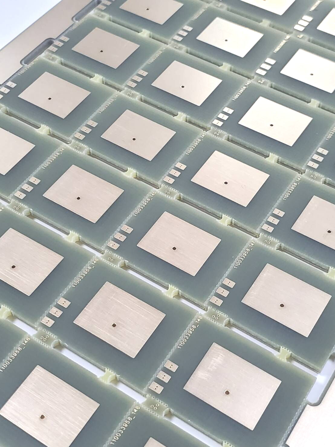
- 4L HDI PCB, Isola DE104 material, 2.1mm Thickness, 1/0.5/1/1oz Cu, Immersion Gold(2u")
- Number of Layers: 4L
- Board Thickness: 2.1mm
- Surface Treatment: Immersion gold(2u")
-
 See details
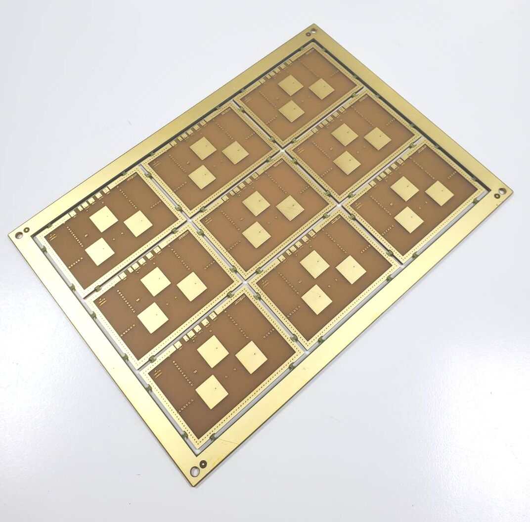
- 4L HDI PCB, Isola DE104 material, 2.3mm Thickness, 1/0.5/1/1oz Cu, LPI, Immersion Gold(2u")
- Number of Layers: Four layers
- Board Thickness: 2.3mm
- Surface Treatment: Immersion gold(2u")
-
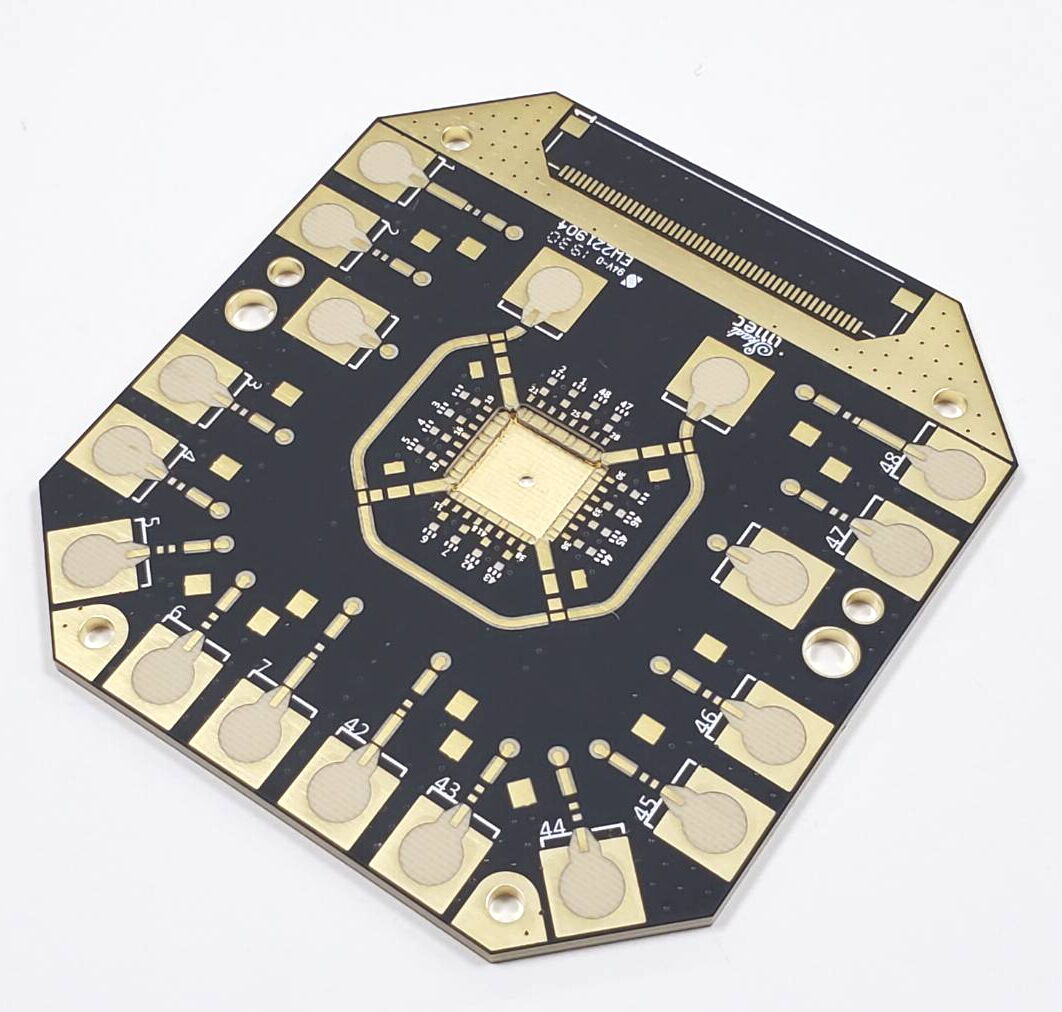 See details
- 6L HDI PCB, Isola I-Tera MT40, 1oz Cu, LPI(Black), ENEPIG, Blind vias L1-L4
- Number of Layers: Six layers
- Board Thickness: 1.6mm
- Surface Treatment: ENEPIG
-
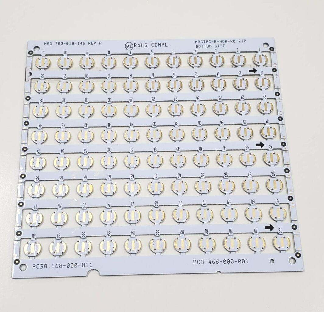 See details
- 3L HDI PCB by Panel Array with FR4 Base Material and 1.0mm Thickness, 2oz Cu, Blind vias: L1-L2
- Number of Layers: Three layers
- Board Thickness: 1.0mm
- Surface Treatment: Immersion gold(3u")
-
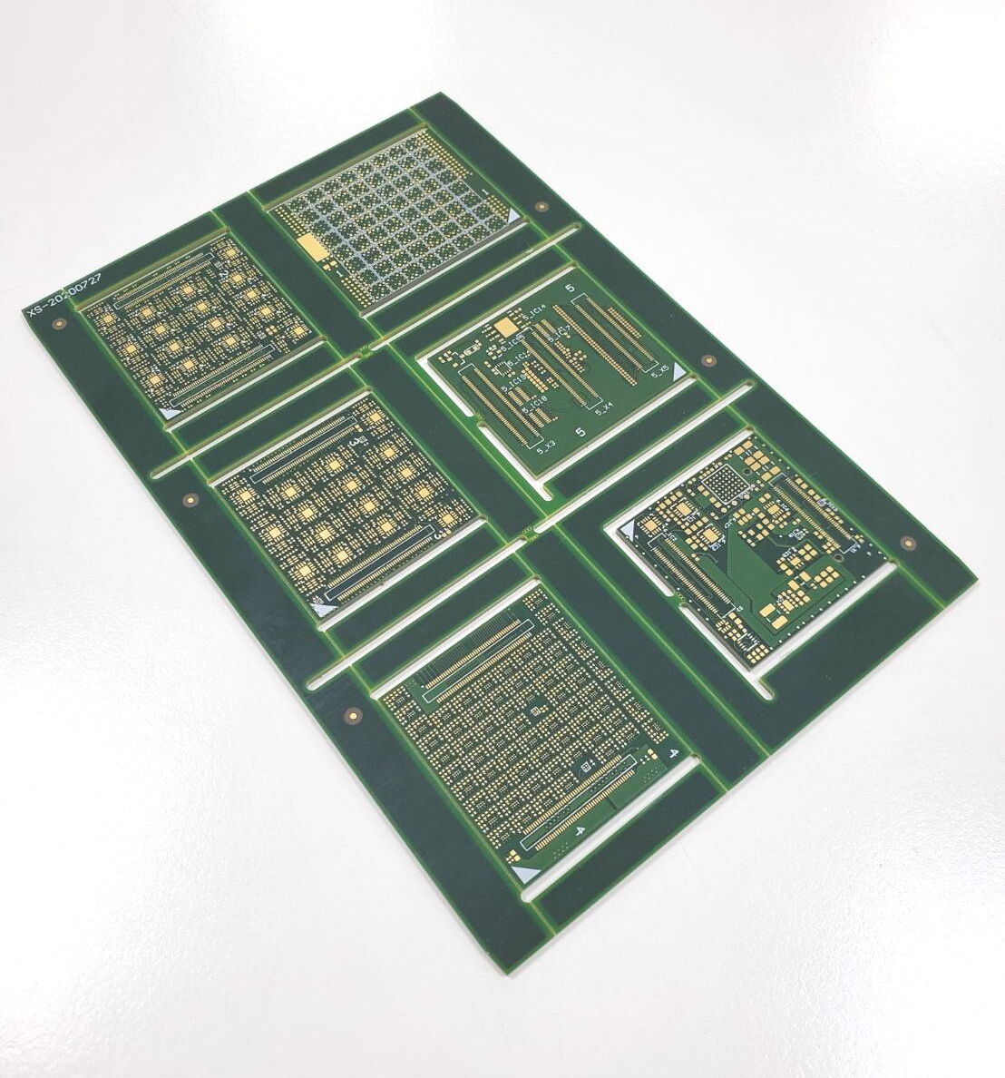 See details
- 10L HDI PCB, FR4(TG170), 1oz Cu,LPI, Immersion Gold(2u"),Impedance control
- Number of Layers: 10 layers
- Board Thickness: 1.55mm
- Surface Treatment: Immersion Gold(2u")
-
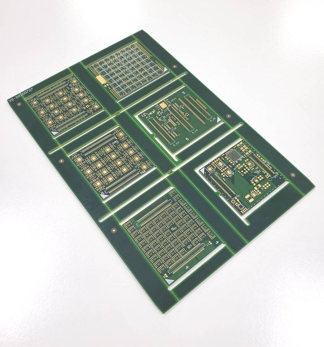 See details
- 10L HDI PCB, FR4(TG170), 1oz Cu,LPI, Immersion Gold(2u"), Impedance control
- Number of Layers: 10L
- Board Thickness: 1.55mm
- Surface Treatment: Immersion Gold(2u")
-
 See details
- 4 Layers 1-Level HDI Medical Display PCB
- Number of Layers: 4 Layers
- Board Thickness: 1.0mm
- Surface Treatment:

Contact Us