


Sorry, no sales person is available right now to take your call. Pls leave a message and we will reply to you via email as soon as possible.
Heavy Copper PCB Design Guide: High Power Solutions
2025-12-16
As power electronics in EVs and industrial sectors demand higher currents, standard PCBs fall short. This guide explores how Heavy Copper PCBs act as 'energy arteries,' offering a comprehensive roadmap from current calculations to DFM strategies for achieving maximum reliability and thermal performance.
The Unique Value of Heavy Copper PCBs
The core advantage of Heavy Copper PCBs (defined as copper thickness ≥3oz, where 1oz ≈ 35μm) lies in their superior current carrying capacity and thermal management.
For instance, in EV charging stations, power modules must sustain currents exceeding 100A. Standard PCBs would suffer from rapid temperature spikes due to Joule heating, leading to performance degradation or failure. Heavy copper boards, with their low resistance, not only conduct current efficiently but also act as integrated heat sinks, dispersing heat to prevent hotspots.
Structural Integrity: The additional copper thickness acts like a steel reinforcement for the board, increasing:
- Flexural strength by approximately 30%
- Vibration resistance by approximately 25%
This makes them ideal for harsh industrial environments and automotive applications where mechanical stress is a concern.
The Golden Rules of Heavy Copper Design
1. Scientific Selection of Copper Thickness
Principle: "Current-Driven, Precision Matching." Avoid the misconception that "thicker is always better." Blindly increasing thickness drives up costs and introduces manufacturing risks like uneven etching or soldering defects.
Practical Form ula for Current Capacity
A rule of thumb for estimating allowed current (Environment ≤40℃):
Current (A) ≈ Copper Thickness (oz) × Trace Width (mm) × 0.8
Note: For precise calculations regarding temperature rise and conductor sizing, we recommend adhering to the IPC-2221 Generic Standard on Printed Board Design. Alternatively, you can verify your specific parameters using an industry-standard PCB Trace Width Calculator.
Application Example
- Spec: 3oz Copper + 3mm Trace Width
- Capacity: ≈ 7.2A
- Verdict: Sufficient for most industrial power supply applications.
KINJI Engineering Advice
- Sweet Spot: Prioritize mainstream specs between 3oz and 6oz.
- Risk Zone: Exceeding 10oz can lead to board warping and drilling difficulties. Avoid over-design unless strictly required (e.g., aerospace).
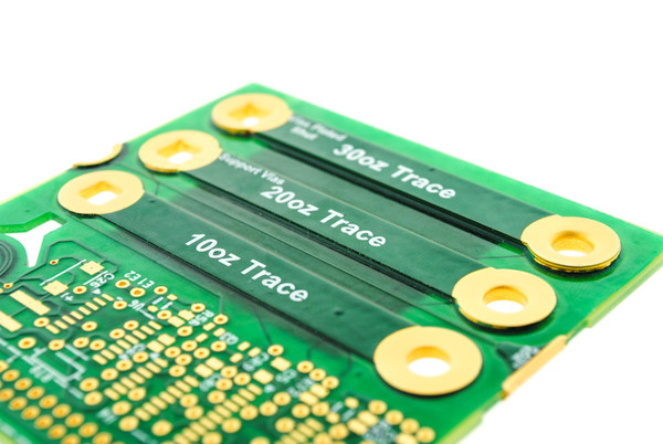
Figure 1. Sample featuring 2oz, 10oz, 20oz, and 30oz copper features on the same layer
2. Trace Design: Ensuring Smooth Transmission
Width Specifications-
- 3oz Copper: Min trace width ≥0.3mm (approx 12 mil).
- 6oz Copper (at 10A): Recommended width ≥5mm.
Transition Design
- Avoid abrupt necking (sudden narrowing/widening).
- Use tapered transitions (length ≥ 3x the width difference) to prevent "current bottlenecks" and localized heating.
Thermal Optimization
- Utilize copper pouring + thermal vias under high-power components.
- Via Specs: Diameter 0.8-1.2mm; Pitch 2-3mm to promote heat transfer to ground/power planes. For advanced thermal modelling, refer to the guidelines on Thermal Management in Power Electronics.
3. Via Design: Addressing Key Pain Points
Hole Size: Minimum diameter ≥0.8mm for 3oz copper to ensure plating quality.
Plating Thickness: Hole wall copper should be ≥20μm (IPC Class 2/3 standard).
Current Distribution:
- Never rely on a single via for high-current paths.
- Rule of Thumb: For 5A current on 3oz copper, use 2-3 vias in parallel (stitching vias). Assume 2-3A capacity per via.
Solder Mask:
- Ensure sufficient solder mask clearance (opening).
- Opening size should be 0.2-0.3mm larger than the pad to prevent mask ink from entering the hole and affecting soldering.
DFM (Design for Manufacturing) Critical Considerations
To ensure your design is manufacturable at scale, pay attention to these four factors:
1. Etching Process Optimization
Due to the "undercut" effect in etching thick copper:
Trace/Space (W/S):
- 3oz: Min W/S ≥0.3mm (12 mil).
- 6oz: Recommended W/S ≥0.4mm (16 mil).
Copper Pouring:
- Use Cross-hatched (Grid) pouring for large areas to prevent blistering.
- Grid settings: Spacing 2-3mm, Line width 0.2-0.3mm.
- If solid pour is necessary, include venting slots (width 0.5mm) to release stress.
2. Lamination and Stack-up
Symmetry: Place heavy copper layers symmetrically around the center of the stack-up to prevent bow and twist.
Material Selection: Always use High-Tg materials (Glass Transition Temperature ≥170℃), such as FR-4 Tg170 or Polyimide, to withstand the thermal stress of heavy copper fabrication and assembly.
3. Soldering & Assembly Adaptation
Component Selection: Prefer robust packages like TO-220 or D2PAK. Avoid soldering small passives (0402/0603) directly onto heavy copper planes.
Pad Design: Enlarge pads by 0.2-0.3mm compared to standard designs. (e.g., 0805 pads should increase from 0.8x1.2mm to 1.0x1.5mm).
Reflow Profile:
- Increase peak temperature by 5-10℃.
- Extend soaking time by 10-15 seconds to prevent cold solder joints due to the high thermal mass of the copper.
4. Cost Optimization Strategy
Hybrid Build-up: Use 1-2oz for logic/signal areas and restrict heavy copper only to critical power paths to avoid over-design.
Standardization: Stick to standard board thicknesses (1.6mm, 2.0mm). Non-standard thicknesses (>3.0mm) significantly increase material costs.
Early Engagement: Consult with KINJI's CAM engineers before finalizing the design to confirm min/max specs for etching and drilling.
Summary
Successful Heavy Copper PCB design relies on three pillars:
- Precise Specification: Choosing 3-6oz based on actual current needs.
- Risk Mitigation: Implementing tapered traces, parallel vias, and proper spacing.
- DFM First: Prioritizing etching, lamination, and soldering requirements early in the design phase.
Although thick copper PCB design is challenging, focusing on two core principles—efficient current conduction and full process compatibility—allows you to meet demanding performance targets while ensuring manufacturability and avoiding common design pitfalls in high‑power applications.
Need assistance with your high-power project? KINJI Group specializes in Heavy Copper PCBs for automotive and industrial applications.
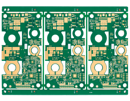
Figure 2. KINJI Heavy Copper Board PCB Product Example
Last updated: December 2025
© KINJI Group – Powering the future, one reliable substrate at a time.
Previous Article: Managing PCB Warpage in Embedded SiC Modules (2025)
Next Article: Heavy Copper PCB Design Guide: High Power Solutions
trending news
Contact Us