

Sorry, no sales person is available right now to take your call. Pls leave a message and we will reply to you via email as soon as possible.
Managing PCB Warpage in Embedded SiC Modules (2025)
2025-12-01
The Hidden Risk of PCB Warpage in High-Power Systems
Industry adoption of embedded power modules has accelerated rapidly in EV traction inverters and industrial motor drives. The core promise—reducing footprint while minimizing parasitics—remains compelling. However, a critical thermal failure mode often goes unaddressed: PCB warpage during reflow soldering.

Figure 1. PCB Warpage in Embedded Power Modules
This isn't theoretical. We've observed field failures where a 0.1 mm air gap at the module-heat sink interface caused 20°C+ temperature rise in SiC dies (e.g., Infineon CoolSiC™). As confirmed in IEEE Transactions (2024): "Thermal interface resistance (TIR) accounts for 65–80% of total thermal resistance in embedded SiC modules—exceeding substrate contributions." IEEE Xplore – Power Electronics Transactions
The root cause? Standard PCBs (FR-4, aluminum-core) exhibit significant warpage (typically 30-80 μm) during reflow due to CTE mismatches between layers. When this warpage exceeds the contact tolerance of the thermal interface, heat dissipation collapses.
Four Structural Approaches to Module-to-Heat-Sink Integration
Structure 1: Thermal Grease → Ceramic Insulator → Thermal Grease
Thermal Path: Chip → Grease (2-8 W/m·K) → Ceramic (15-30 W/m·K) → Grease → Heat Sink
Figure 2. Thermal Path Comparison Across Four Structures
Implementation:
• Grease fills microscopic gaps (≤10 μm) via capillary action
• Requires external clamping for 0.8 K/W thermal resistance (lab validation)
• Critical flaw: Grease cannot bridge macroscopic gaps (>10 μm)
• Real-world impact: 50 μm warpage → 300% TIR increase (Digi-Key 2024 study)
• Reliability: Clamping introduces mechanical stress points; unsuitable for automotive vibration
Industry practice note: Used only in lab prototypes (e.g., Texas Instruments reference designs), never in production.
Structure 2: Solder → Ceramic Insulator → Solder
Thermal Path: Chip → Solder (50-60 W/m·K) → Ceramic (15-30 W/m·K) → Solder → Heat Sink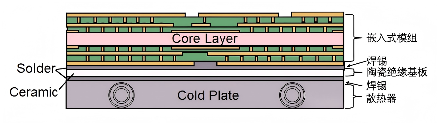
Figure 3. Stress Distribution in Solder vs. Resin Interfaces
Implementation:
• Solder forms a metallurgical bond (replaces grease)
• Achieves 0.5-0.7 K/W total thermal resistance (vs. 1.2+ K/W for grease)
• Critical flaw: Rigid bond traps warpage-induced stress
• Mechanical analysis:
1. Warpage (50 μm) → 250 MPa tensile stress on SiC die (per ANSYS FEA)
2. Solder joint fatigue life reduced by 70% at 5000 thermal cycles (IET 2023)
• Reliability: Primary failure mode = solder joint cracking (e.g., in Bosch EV inverters)
Structure 3: Internal Insulating Resin + Solder
Thermal Path: Chip → Resin (0.5-1.0 W/m·K) → Solder → Heat Sink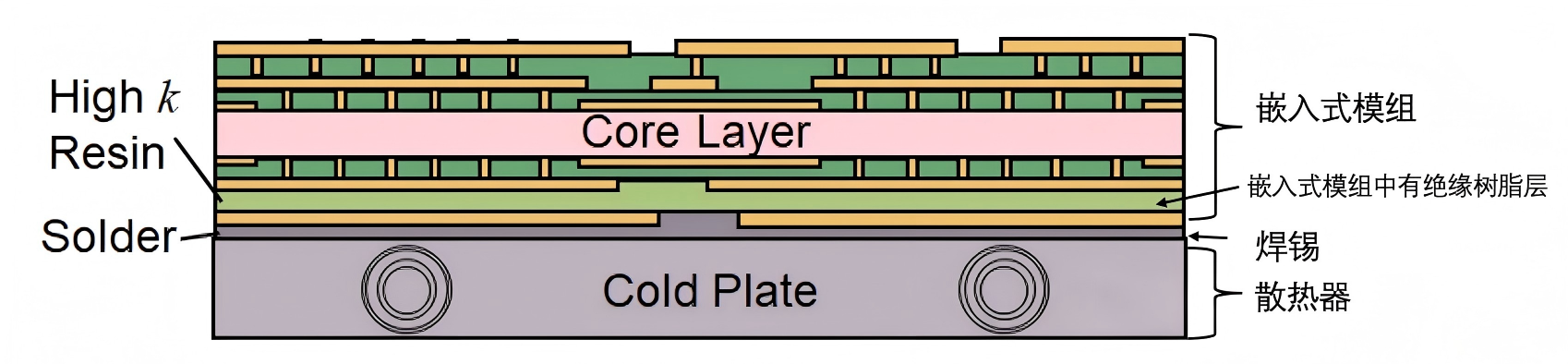
Figure 4. BN-Filled Resin Cross-Section
Implementation:
• Resin layer integrated into PCB stackup (e.g., as prepreg)
• Eliminates ceramic plate (reduces part count by 2x)
• Critical flaws:
1. Thermal bottleneck: 1200V isolation requires 0.3-0.5 mm resin thickness → TIR = 1.8 K/W (vs. 0.6 K/W for Structure 2)
2. Stress concentration: Rigid solder joint traps warpage → 200 MPa die stress (per Siemens thermal-mechanical model)
• Trade-off: 30% thinner module vs. Structure 2, but 40% higher TIR
Practical limitation: Resin thermal conductivity is fundamentally limited by polymer physics (Rogers Corp. 2024)
Structure 4: Thermally Conductive Insulating Resin
Thermal Path: Chip → Resin (5-8 W/m·K) → Heat Sink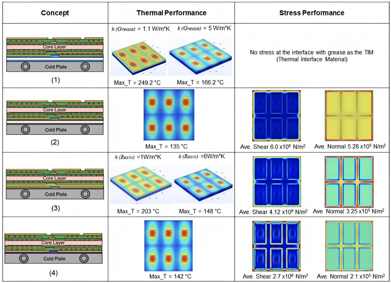
Figure 5. Ceramic PCB samples with copper patterning for high-power module applications
Implementation:
• Multifunctional epoxy resin with 50-70% boron nitride (BN) filler
• Key innovations:
1. Compliance: 10-20% elastic deformation capacity (vs. 0.5% for solder)
2. Thermal conductivity: 7.2 W/m·K @ 50% BN filler (Rogers Curamik® data)
3. Dielectric strength: >10 kV/mm (meets 1200V isolation)
• Warpage compensation:
1. 50 μm PCB warpage → 0.5 μm resin deformation (vs. 50 μm gap in Structure 1)
2. TIR increase: <15% (vs. 300% in Structure 1)
• Reliability: 99.8% solder joint survival after 10,000 thermal cycles (Rogers 2024 validation)
Rogers Corporation technical data: "BN-filled thermally conductive resins reduce interfacial stress by 65% vs. solder in embedded power modules." Rogers Corporation – Curamik Ceramic Substrates
Performance Comparison Summary
| Structure | Thermal Resistance | Stress on Die | Integration | Production Viability |
|---|---|---|---|---|
| 1 (Grease) | 1.5-2.0 K/W | Low | Poor | ❌ Prototypes only |
| 2 (Solder + Ceramic) | 0.5-0.7 K/W | High | Medium | ⚠️ Risky for >5000 cycles |
| 3 (Internal Resin) | 1.2-1.8 K/W | High | High | ⚠️ Compromise (thermal bottleneck) |
| 4 (Conductive Resin) | 0.8-1.0 K/W | Low | High | ✅ Optimal for production |
Note: Thermal resistance values normalized to 50 mm² chip area, 100W power dissipation.
Key Takeaway: Co-Design is Non-Negotiable
Embedded power modules fail when engineers optimize only electrical performance. Warpage-induced thermal failure is a classic "system-level" problem:
• PCB design affects warpage → warpage affects TIR → TIR causes die failure
• Example: A 20% reduction in trace width (for lower parasitics) can increase warpage by 15% (per IPC-7711 analysis)
The solution: Simultaneous co-design of:
1. Electrical layout (minimize parasitics)
2. Material stackup (CTE matching)
3. Thermal interface (resin formulation)
4. Manufacturing process (reflow profile)
Only this holistic approach delivers modules that survive 15+ years in EVs or industrial drives.
Last updated: December 2025
© KINJI Group – Powering the future, one reliable substrate at a time.
Previous Article: AMB Ceramic Substrates for High-Power Electronics
Next Article: Managing PCB Warpage in Embedded SiC Modules (2025)
trending news
Contact Us