

Sorry, no sales person is available right now to take your call. Pls leave a message and we will reply to you via email as soon as possible.
Detailed Explanation of PCB Special Processes and Their Application Scenarios
2025-03-24
Special PCB Manufacturing Processes and Their Application Scenarios
Special PCB manufacturing processes refer to non-standard techniques adopted to meet specific functional or performance requirements. Below are common special processes and their application scenarios:
I. Signal Integrity-Related Processes
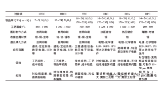
1. Impedance ControlCore Principle: Precisely calculate PCB trace width, dielectric layer thickness, and dielectric constant to control transmission line impedance (e.g., 50Ω, 90Ω, 100Ω), ensuring impedance matching with components.Design Considerations:Stack-up Design: Adjust dielectric thickness (e.g., PP prepreg) and copper weight to meet impedance targets.Material Selection: High-frequency laminates (e.g., Rogers 4350B) minimize dielectric constant (Dk) variations.Simulation: Validate with SI tools (HyperLynx, ADS) to prevent signal reflection/attenuation.Applications: High-speed digital circuits (DDR, PCIe), RF circuits (5G antennas, microwave communication).
2. Advanced Stack-up StructuresTechniques:Symmetrical Stack-up: Reduces thermal deformation (e.g., 2+4+2 for 8-layer boards).Hybrid Dielectric Stack-up: Combines FR-4 with high-frequency materials (e.g., PTFE) for optimized signal/power layer distribution.Embedded Capacitor/Resistor Layers: Integrates passive components internally to reduce surface components.EMC Optimization:"Signal-Ground-Signal" layer sequence to suppress crosstalk.20H rule (power layer indented 20× dielectric thickness) to reduce edge radiation.Applications: Server motherboards, automotive radar modules, aerospace systems.
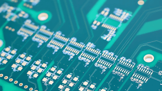
II. High-Density Interconnect (HDI) Processes
1. Blind/Buried ViasProcess Details:Laser Drilling: CO₂/UV lasers create micro-vias (50–100μm).Via Filling: Conductive paste or copper plating ensures interlayer connectivity.Design Advantages:Shortens signal paths, improves high-frequency SI (reduces via stub effects).Supports high-density routing under BGAs (e.g., 0.4mm pitch escape routing).Typical Stack-ups: 1+N+1 (blind vias), 2+N+2 (any-layer HDI).
2. Counterbore HolesFabrication:Step-drilling with flat drills or CNC milling to create stepped holes.Hole diameter > standard vias, depth = 50–80% of board thickness.Applications:Securing countersunk screws for PCB-enclosure mounting (industrial controls).Eliminates surface protrusions for ultra-thin devices.
III. Special Materials & Surface Finishes
1. Heavy Copper PCBsSpecifications:Copper Weight: 2–20oz (70–700μm outer layers; up to 200oz inner layers).Etch Compensation: Differential etching controls undercutting.Thermal Design:Direct heat dissipation via copper layers (e.g., TO-220 heatsinks soldered to copper).Supports >100A current (e.g., EV motor controllers).Applications: Power modules, solar inverters, grid systems.
2. Electroplated Ni/Au & Gold Fingers
| Type | Au Thickness | Wear Resistance | Cost | Applications |
|---|---|---|---|---|
| Electroplated Hard Gold | 0.5–1.5μm | Very High | High | Gold fingers, RF connectors |
| ENIG | 0.05–0.2μm | Moderate | Medium | BGA pads, standard solder joints |
Key Parameters:Hardness: ≥200 HV (hard gold).Durability: ≥10,000 cycles (PCIe compliance).
ENEPIG (Electroless Ni/Pd/Au)Layer Structure:Ni (3–5μm) → Pd (0.05–0.1μm) → Au (0.03–0.05μm).Advantages:Compatible with wire bonding and soldering.Pd layer prevents Ni migration (enhances reliability for high-frequency signals).Applications: Automotive ECUs, satellite modules, medical implants.
IV. Special Processing Techniques
3D Structured PCBs
- Implementation:Flexible Bending Zones: Laser-cut or stamped foldable areas (e.g., foldable phone hinges).3D Assembly: Stacked PCB modules via connectors (e.g., TWS earbud charging cases).
- Validation:ANSYS Mechanical for stress analysis.Thermal cycling tests (-40°C to 125°C, 1,000 cycles).
V. Process Selection Guidelines
- Consumer Electronics:HDI + impedance control (smartphone motherboards) + ENIG finish.
- Automotive Electronics:Heavy copper (power modules) + ENEPIG (ECUs) + high-Tg materials (heat resistance).
- Aerospace:Polyimide rigid-flex PCBs + gold fingers + X-ray inspection.
This translation preserves technical accuracy while adhering to industry-standard terminology and documentation practices.
trending news
Contact Us