

Sorry, no sales person is available right now to take your call. Pls leave a message and we will reply to you via email as soon as possible.
High Temperature, High Power, Long Lifespan: Why AMB Ceramic Substrates Are the Ideal Match for Third-Generation Semiconductors
2025-10-28
In demanding applications such as EV fast charging and photovoltaic inverters, power modules face two critical challenges: sudden thermal spikes that can trigger device failure, and long-term material fatigue caused by daily temperature swings and harsh environments. These factors directly limit performance and service life.
To address these issues, the industry is turning to AMB (Active Metal Brazing) ceramic substrates. By creating a robust metallurgical bond between ceramics and metals, AMB substrates combine the high thermal conductivity and insulation of ceramics with the electrical and mechanical advantages of copper. The result is a substrate that delivers both functional integration and long-term reliability.
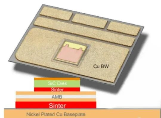
Figure 1. SiC Power Module with AMB Substrate
Why AMB Ceramic Substrates Matter in High-Power Electronics?
Power devices require substrates that can simultaneously provide efficient heat dissipation, mechanical strength, and electrical insulation. This is where ceramics such as aluminum nitride (AlN) and silicon nitride (Si₃N₄) excel. However, when paired with copper, a major challenge arises: thermal expansion mismatch.
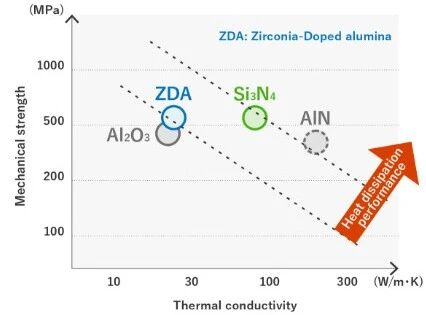
Figure 2. Mechanical Strength vs. Thermal Conductivity of Ceramics
| Material | Thermal Expansion Coefficient (CTE) |
|---|---|
| Copper | ~17 ppm/°C |
| Aluminum Nitride (AlN) | ~4.5 ppm/°C |
| Silicon Nitride (Si₃N₄) | ~2.8 ppm/°C |
This mismatch generates significant stress at the interface during temperature cycling, often leading to delamination, copper lift-off, or ceramic cracking. Traditional DBC (Direct Bonded Copper) technology cannot fully resolve this issue. AMB, by contrast, introduces a reactive brazing layer that chemically bonds copper to ceramic, eliminating the mismatch problem at its source.
The AMB Manufacturing Process: Three Key Stages
1. Pre-Treatment and Paste Application: Ceramic substrates and copper foils are cleaned and micro-etched to improve adhesion. A silver-copper-titanium (Ag-Cu-Ti) brazing paste is then applied and dried to form a stable pre-bond layer.
2. Vacuum Brazing: The assembly is heated to 800–1000°C in a vacuum or reducing atmosphere. Titanium in the brazing paste reacts with the ceramic surface, forming a strong transition layer and creating a durable metallurgical bond.
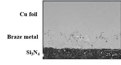
Figure 3. Cross-Sectional SEM of Ceramic–Active Metal–Copper Layers
3. Post-Processing and Quality Control: Circuit patterns are defined through photolithography and etching. Surface finishing, such as electroless nickel/gold plating, enhances solderability and corrosion resistance. Each substrate undergoes rigorous testing, including ultrasonic scanning, X-ray inspection, peel strength measurement, and environmental reliability checks.
Core Advantages of AMB Ceramic Substrates
1. Superior Thermal Management: The combination of thick copper and high-conductivity ceramics enables rapid heat dissipation, preventing localized hotspots and maintaining safe junction temperatures in high-power modules such as EV fast chargers.
2. High Reliability Under Thermal Cycling: The reactive metal layer acts as a stress buffer, absorbing expansion mismatch and preventing delamination or cracking during repeated temperature fluctuations.
3. High Current-Carrying Capacity: AMB substrates support thicker copper layers (≥0.3 mm), providing low-resistance pathways for high current while maintaining efficient heat removal. This enables compact, high-power-density designs.
Quality Standards That Define Reliability
- Bonding Quality: Void rates should remain below 3%, and below 1% for automotive-grade applications. High peel strength ensures copper adhesion under thermal and mechanical stress.
- Conductive Layer Design: Copper thickness must be matched with line width and spacing. Thin copper (0.127 mm) supports fine lines below 0.25 mm for high integration, while thick copper (≥0.4 mm) requires wider spacing (≥0.6 mm) to handle high current safely.
trending news
Contact Us