


Sorry, no sales person is available right now to take your call. Pls leave a message and we will reply to you via email as soon as possible.
Foldable Phones Accelerate Toward Mass Adoption: Behind Hinge Iteration, Why Are FPC and HDI Becoming Core Industry Necessities?
2026-09-22
Foldable phones are accelerating from a high-end niche segment toward large-scale adoption. According to public information, in September 2026, three flagship models—Huawei Mate XT2, Xiaomi 18 Fold, and iPhone Duo—were released within 72 hours, priced at 19,999 yuan, 10,999 yuan, and 15,999 yuan, respectively, covering the high-end ten-thousand-yuan price band. This marks the increasing maturity of the foldable form factor and a significant acceleration in the iteration pace of leading brands. According to IDC forecasts, global foldable phone shipments will reach 22.9 million units in 2026, up 12.6% year-on-year, as the industry officially enters a stage of normalized, large-scale growth.
On the consumer side, users focus primarily on screen form factor, hinge feel, and body thinness and lightness. From the perspective of the PCB (printed circuit board) industry chain, however, the essential innovation of foldable phones lies in the systematic reconstruction of the device's physical structure and underlying circuit system. Unlike the static, fixed circuit layout of bar phones, foldable phones rely on precision hinges to achieve hundreds of thousands of high-frequency open-and-close cycles, requiring internal circuits to deeply adapt to three demanding operating conditions: dynamic bending, extreme space compression, and highly stable signal transmission. Against this backdrop, FPC (flexible printed circuit) and HDI (high-density interconnect) boards have evolved from conventional supporting components into core enabling technologies that support the thinness, high reliability, and long-life iteration of foldable phones; at the same time, rigid-flex boards and high-density SMT (surface mount technology) processes have become key supports for the mass production of high-end models.
As the core structure in continuous motion within the device, the hinge is the primary constraint source for PCB design and manufacturing. Its extremely small bending radius, narrow cavity space, high-frequency reciprocating motion, and dynamic stress transmission characteristics directly define the material standards, structural design, and process precision of the FPC passing through the hinge and the HDI mainboard positioned adjacent to the hinge. From the supply chain perspective, this constraint has already translated into quantifiable industrial collaboration.

I. FPC: Adapting to Dynamic Hinge Bending, Building the Foundation of Device Reliability
In mainstream foldable phone solutions, FPC is the dynamic circuit carrier running through the interior of the hinge, carrying core signal transmission tasks such as display, touch, power supply, and RF. It must follow the hinge through hundreds of thousands of repeated bending, stretching, and micro-twisting cycles. Unlike ordinary FPC, which only needs to meet basic flexibility requirements, the core difficulty of foldable-phone-specific FPC lies in electrical stability and structural fatigue resistance under long-term cyclic deformation, which is also the key factor determining the service life of the device.
1. Material Selection: Fatigue Resistance and Stress Adaptation
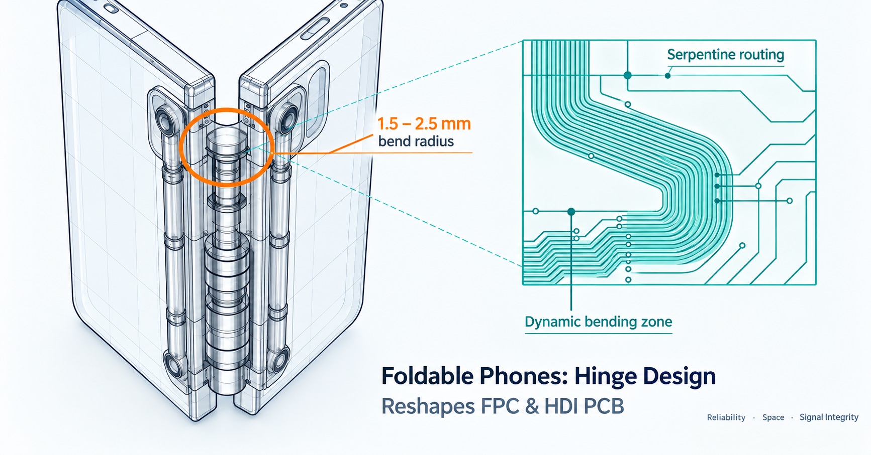
The hinge bending radius of mainstream flagship foldables is only 1.5–2.5 mm, and the device must pass more than 200,000 open-and-close reliability tests. To avoid failure issues such as copper foil cracking, micro line breakage, and interlayer delamination caused by long-term bending:
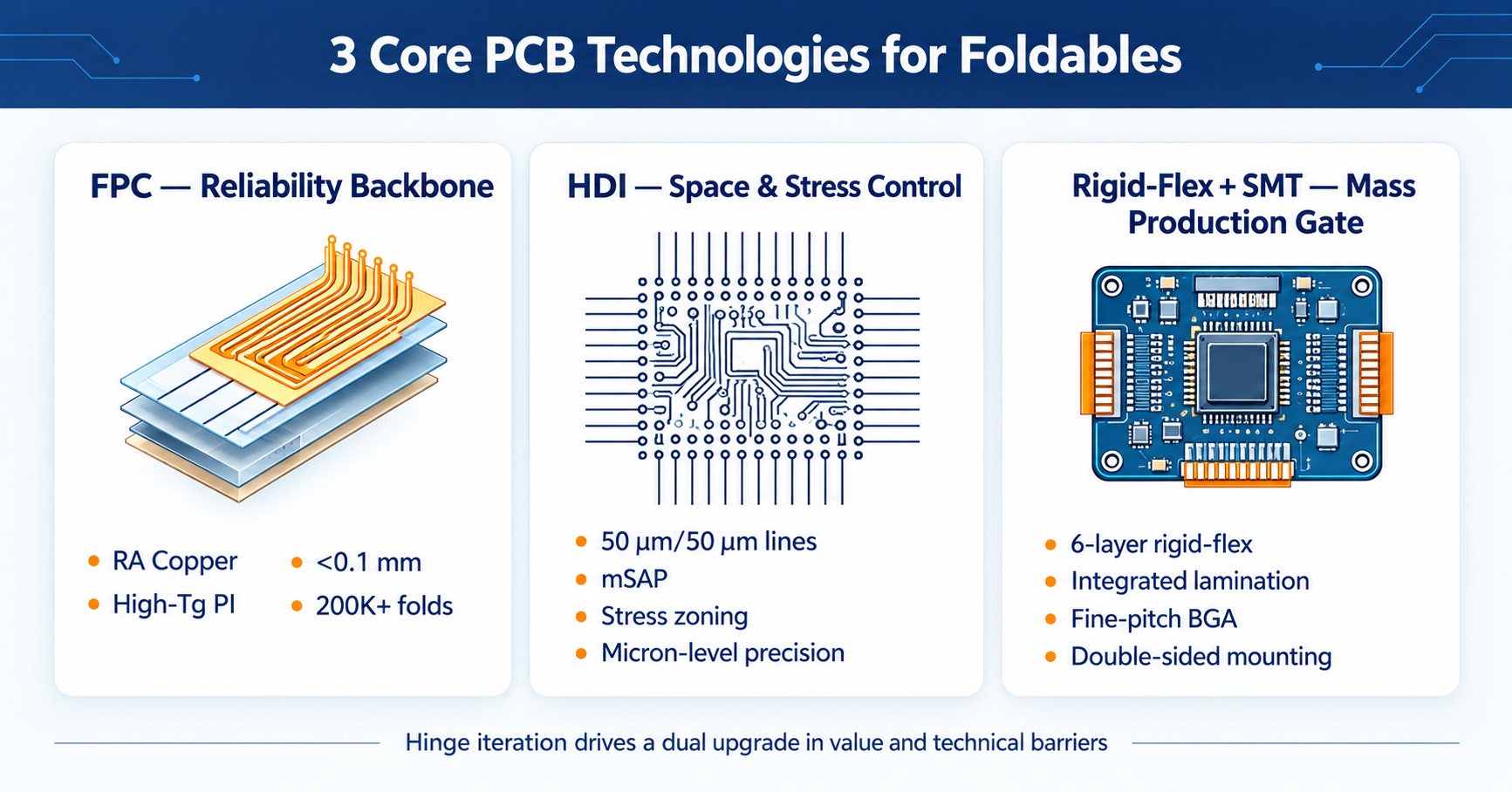
Conductor material: The industry generally uses high-performance rolled annealed copper (RA copper) with stronger fatigue resistance. Compared with ordinary electrolytic copper, its bending life is increased by more than 3 times; at the same time, copper foil surface roughness is strictly controlled (Ra ≤ 0.2 μm), inhibiting the initiation and propagation of microcracks at the source.
Substrate combination: High-Tg (glass transition temperature) modified PI (polyimide) film is used to adapt to dynamic stress and high-low temperature alternating conditions, ensuring dimensional stability during long-term use.
Industry evidence: Related products from FPC manufacturers such as Avary Holding and Honflex Electronics have successfully supplied mainstream foldable phone terminals, and the gross margins of related businesses rose year-on-year in the first half of that year, indirectly confirming the trend of value enhancement of high-end bend-resistant FPC in the foldable phone supply chain.
2. Structural Lamination: Ultra-Thin Design with Gradient Stiffness
The multi-link transmission structure of the hinge extremely compresses the internal wiring space, and the industry generally adopts an ultra-thin adaptation scheme with gradient stiffness:
Core bending zone: A single-layer ultra-thin lamination of "8 μm copper foil + 12.5 μm PI substrate" is used to minimize bending stress and improve deformation freedom.
Transition zone: A gradient double-layer structure is used at the hinge inlet and outlet to balance wiring density and structural strength, avoiding stress concentration fractures caused by abrupt soft-hard structural changes.
Overall thickness: By streamlining redundant adhesive layers and reinforcement structures, the total thickness of the FPC in the hinge section is strictly controlled within 0.1 mm, effectively alleviating opening/closing jamming and extrusion deformation.
3. Electrical Performance and Protective Integration
Routing and interference resistance: In response to the irregular stress generated by hinge opening and closing, the FPC adopts serpentine detour routing and 0.1 mm-class ultra-fine equidistant line spacing design to proactively reserve deformation margin. For MIPI high-speed display signals and RF signals, a "ground-signal-ground" coplanar waveguide structure is used to precisely control line impedance under dynamic bending conditions, ensuring continuity and integrity of signal transmission during the opening and closing process.
Rigid-flex transition and sealing: The transition section between the rigid mainboard and the flexible hinge zone is a high-incidence area for device failure. The industry uses high-precision lamination processes to achieve smooth transition of rigid-flex material modulus, reducing interlayer gaps and resisting continuous pulling caused by micro-motion of the hinge; combined with high-fit-precision coverlay to achieve full-area sealing, effectively reducing wear on circuits caused by dust and friction debris inside the hinge.
II. HDI: Breaking Through the Dual Constraints of Space and Stress, Enabling High-Density Circuit Integration
Although the HDI mainboard does not directly participate in bending, the centered layout of the foldable phone with the hinge as the core greatly squeezes the internal space of the body. Coupled with stacking limitations from flexible screens, high-capacity batteries, and multi-module imaging systems, the mainboard layout area is extremely compressed; at the same time, vibration and micro-deformation generated by hinge opening and closing are continuously transmitted to the surrounding body, creating persistent stress interference. The dual constraints of scarce space and dynamic stress make HDI the core solution for miniaturized, highly integrated, and highly stable circuit design in foldable phones.
Three Core Challenges in Foldable Phone HDI Mainboard Design:
Extreme space utilization: Relying on laser microvias, blind and buried via stacking, and mSAP processes to achieve 50 μm/50 μm line width and spacing.
Stress zoning control: Avoiding micro components and stacked vias in areas adjacent to the hinge, retaining only low-stress routing.
High-precision manufacturing: Strictly controlling interlayer registration and board flatness to ensure micron-level matching with the hinge and FPC.
High-density routing: Relying on advanced processes such as laser microvia processing, blind and buried via stacking, and sequential lamination, HDI can achieve ultra-fine 50 μm/50 μm line width and spacing. Without increasing the number of mainboard layers or thickness, it efficiently completes circuit interconnection for SoC, memory, RF, power management, and other modules.
Structured stress zoning layout: In stress-sensitive areas adjacent to the hinge, blind and buried via stacking structures, precision micro components, and dense crossing lines are in principle prohibited, and only low-stress general routing is retained, structurally avoiding board micro-deformation, line breakage, and solder joint cold joints caused by deformation.
Micron-level manufacturing precision: The assembly tolerance between the foldable hinge and the mainboard is extremely low, and micron-level deviation can cause opening/closing jamming or assembly interference. This requires HDI to strictly control the consistency of interlayer registration, laser drilling, electroplating via filling, and exposure etching throughout the process, ensuring board flatness, preventing warpage and deformation, and achieving precise matching with FPC connector points and hinge structures.
III. Rigid-Flex Boards + High-Density SMT: Completing the Mass Production Capability for Foldable Phones
1. Rigid-Flex Boards: The Technical High Ground of Integrated Assembly
A rigid-flex board is not a simple splicing of rigid boards and flexible boards, but an integrated solution that deeply combines the rigid requirements for component mounting with the flexible bending requirements of hinge opening and closing. Because soft and hard substrates differ significantly in mechanical properties and coefficient of thermal expansion (CTE), the entire process of lamination, drilling, electroplating, and shaping is highly prone to deformation, interlayer misalignment, and interface delamination, making it one of the core difficulties in foldable phone PCB mass production.
Mass production validation case: An international first-tier consumer electronics brand adopted a customized 6-layer blind and buried via rigid-flex board solution in its flagship foldable phone. By optimizing the rigid-flex transition design in the hinge area, it effectively solved the solder joint fatigue problem caused by repeated opening and closing, and the device successfully passed 200,000 folding tests.
Solution architecture innovation: On the PCB manufacturing platform, the 6-layer HDI rigid-flex board launched by Kinji Group adopts integrated lamination molding ("4-layer HDI rigid board + 2-layer flexible board"), replacing the traditional split architecture of "rigid PCB + independent FPC + connector." This solution reduces the extra thickness and signal loss caused by connectors, and introduces a dedicated stress release design in the rigid-flex boundary area, greatly improving bending resistance stability.
2. High-Density SMT: The Final Step of High-Precision Assembly
On the basis of high-density upgrades to PCB substrates, high-density SMT processes are the final guarantee for performance realization. While the mainboard area of foldable phones shrinks, device integration density increases significantly, and fine-pitch BGA, micro passive components, and double-sided high-density mounting have become standard configurations. Precision assembly in a narrow space places extremely high demands on solder paste printing uniformity, component alignment accuracy, reflow soldering temperature profile control, and AOI (automated optical inspection) precision. Minor deviations in the PCB process will be amplified in the SMT stage, directly affecting mass production yield and terminal usage stability.

IV. Industry Summary: Hinge Iteration Drives Comprehensive Value Upgrade Across the PCB Industry Chain
Taken together, the growth of the foldable phone market is not merely an increase in shipment volume, but drives a dual upgrade in product added value and technical barriers in the PCB industry:
The dynamic motion properties of the hinge: Forcing FPC to evolve toward fatigue-resistant materials, ultra-thin laminations, serpentine routing, and high-reliability protection.
Space squeeze and stress transmission: Forcing HDI to continue iterating toward ultra-high density (mSAP), precision stress zoning, and rigid-flex integration.
Unlike the standardized, static PCB manufacturing model of bar phones, the core competitiveness of foldable phone PCBs lies in the deep adaptation of precision circuit design to dynamic mechanical hinges. From the perspective of the supply chain landscape, companies with full-category coverage of FPC, HDI, and rigid-flex boards, and which have already completed mass production validation in foldable phone scenarios, are becoming key nodes connecting upstream materials and downstream terminals.
As foldable phones continue to evolve toward multi-fold form factors, extreme thinness, and longer lifespans, internal physical space will be further compressed, and circuit integration complexity and dynamic stability requirements will continue to rise. Under this trend, supply chain companies with high-end technical reserves and stable process control capabilities will continue to benefit from the industry dividends brought by the high-end iteration of foldable phones.
trending news
Contact Us