


Sorry, no sales person is available right now to take your call. Pls leave a message and we will reply to you via email as soon as possible.
The True Cost of Custom PCBs: Understanding the Factors that Affect the Bottom Line
2026-09-21
Printed Circuit Boards (PCBs) serve as the core carrier of electronic connection and mechanical support, widely applied in consumer electronics, industrial control, new energy equipment, intelligent hardware and other fields. Custom PCB manufacturing is a highly customized engineering project, where every design parameter, material selection and process standard directly affects the final production cost. Many enterprises and R&D teams face uncontrollable budget expenditure in PCB customization, largely due to insufficient understanding of core cost influencing factors and hidden expenditure links in the production chain.
Core Factors Determining Custom PCB Manufacturing Costs
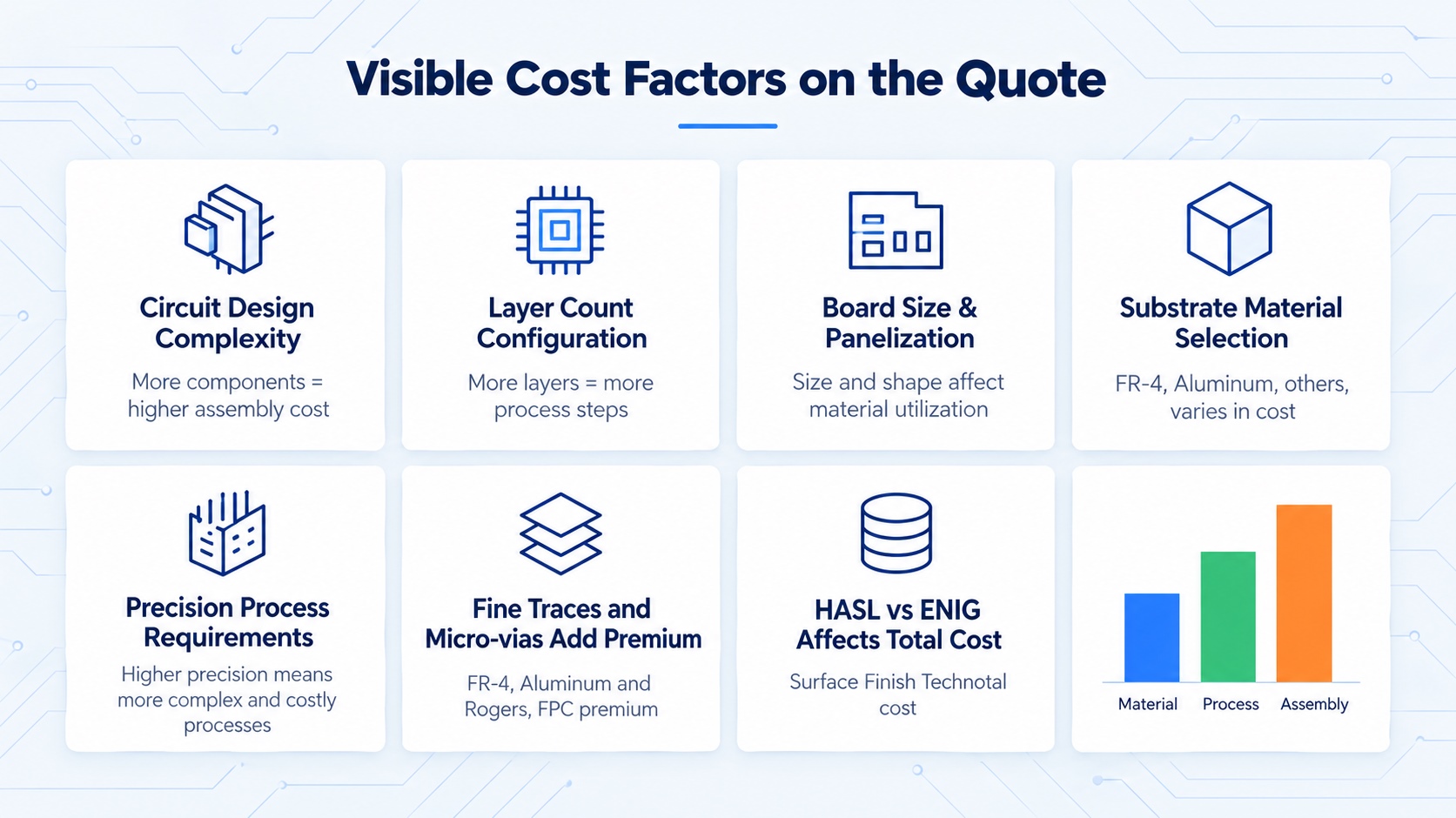
Custom PCB pricing is not a single standardized quotation, but a comprehensive valuation result based on design complexity, process difficulty, material grade and production scale. The core influencing factors are summarized as follows:
1. Circuit Design Complexity
Circuit complexity is the primary factor driving PCB cost changes. High-complexity designs feature dense component layout, intricate circuit routing, and special functional circuits such as high-frequency signal transmission and high-current conduction. Such designs require more precise production processes, stricter quality inspection standards, and longer processing cycles. Meanwhile, complex circuits often need supporting customized assembly solutions, increasing component matching and manual debugging costs. Kinji Group supports high-precision circuit design production including HDI high-density interconnection and embedded copper coin structure, and realizes standardized cost control for complex boards through mature batch processing technology.
2. PCB Layer Count Configuration
The number of board layers is positively correlated with manufacturing cost. Each additional layer requires independent material pressing, circuit etching, lamination and testing processes, which greatly increases raw material consumption and process time. Kinji Group’s mainstream manufacturing capacity covers 1–30 layers of PCBs. Single and double-layer conventional boards adopt standardized batch production with extremely low unit cost; multi-layer boards and high-end HDI multi-layer boards require precision lamination and micro-drilling processes, with corresponding cost increased moderately based on layer count and process difficulty.
3. Board Size, Shape and Panelization Design
Board size and outline shape directly affect material utilization rate and production efficiency. Conventional rectangular PCBs are compatible with automated production lines and standard panelization schemes, with the highest material utilization and lowest processing cost. Irregular, circular, triangular and special-shaped boards require customized tooling and segmented processing, which will generate additional process fees. In terms of size, oversized non-standard boards cannot be integrated into standard production panels, resulting in wasted raw materials and increased unit production costs.
Kinji Group optimizes production efficiency through scientific panelization design. Standardized panel layout can increase material utilization rate to more than 90%, and realizes batch processing of multiple boards in one production cycle, effectively reducing unit manufacturing cost. For special-shaped and customized size boards, the professional engineering team provides targeted panelization optimization schemes to minimize material waste.
4. Substrate and Auxiliary Material Selection
PCB substrate materials vary greatly in performance and price, and material selection must match product application scenarios, which is a key source of cost differentiation. Combined with Kinji Group’s full-range material manufacturing capabilities, the cost levels and applicable scenarios of mainstream materials are as follows:
· Standard FR-4 Material: The most cost-effective universal substrate with stable mechanical and electrical properties, suitable for most consumer electronics, IoT equipment and conventional industrial control circuits. It is Kinji’s mainstream low-cost supporting material, with stable batch production pricing and no extra engineering surcharges.
· High-TG FR-4 Material: Features high temperature resistance and thermal stability, applicable to high-temperature industrial environments and automotive electronic equipment. A small amount of premium is charged on the basis of standard materials, with outstanding cost performance.
· Aluminum/Copper Core Metal Substrate: Has excellent thermal conductivity, suitable for high-power LED lighting, power supplies and new energy power equipment. The material and lamination process are slightly higher in cost than standard FR-4, but can effectively reduce product heat dissipation failure rate.
· Polyimide Flexible Material (FPC): Ultra-thin and highly flexible, applicable to wearable devices, foldable equipment and compact connecting circuits. It requires professional laser profiling technology, with moderate cost and flexible customization capabilities.
· High-Frequency Rogers/PTFE Material: Low dielectric loss and stable signal transmission, specially used for 5G radio frequency, radar and high-speed communication equipment. Due to high-end raw materials and precise impedance control processes, the cost is relatively high, belonging to high-performance customized solutions.
5. Precision Process & Design Specification Requirements
Ultra-precise design parameters will break the standardized production process and generate additional precision processing fees. Conforming to industry universal DFM specifications is the core of cost control. Kinji Group’s standardized low-cost process parameters cover conventional production demands: trace width/spacing ≥5/5mil for ordinary boards, minimum mechanical via drill size ≥0.3mm, standard 1.6mm board thickness and 1oz copper weight. Ultra-fine traces, micro-vias, thick copper customization and non-standard thickness boards all require special process adjustment, bringing additional cost expenditure.
6. Surface Finish Technology Selection
Surface finish determines PCB solderability, oxidation resistance and service life, and is another key factor affecting quotation. HASL (leaded/lead-free) is the most cost-effective universal finish, with excellent solderability and long storage life, suitable for most prototype verification and mass production projects. ENIG and other high-grade finishes feature flat and smooth surface, which is only applicable to high-precision components such as fine-pitch BGA and QFN. Blindly pursuing high-end finishes for conventional designs will cause unnecessary cost waste.
Hidden Costs Easily Overlooked in Custom PCB Projects
In addition to explicit manufacturing fees, there are multiple hidden cost links in the whole cycle from PCB design, prototyping to mass production and delivery, which easily lead to budget overrun:
1. Iterative Prototyping & Testing Costs
Initial design defects often lead to repeated prototyping and performance testing. Each iteration involves material consumption, processing and testing fees, and prolonged R&D cycles will also increase time costs. Kinji Group provides pre-production DFM review and technical simulation services, helping customers optimize design schemes in advance, reduce prototype iteration times, and greatly save R&D trial and error costs.
2. Special Tooling & Process Adjustment Costs
Non-standard design and special-shaped boards require customized production tooling and process parameter adjustment. Frequent tooling replacement and process debugging will increase equipment loss and labor costs. Kinji Group relies on rich manufacturing experience to realize flexible adaptation of most customized designs with existing equipment, reducing additional tooling investment for customers.
3. Assembly & Rework Costs
Unreasonable design and non-standard processes easily cause defects such as solder bridging, empty welding and tombstoning during assembly, resulting in high rework and scrap costs. Kinji’s standardized production process and strict multi-channel quality inspection (AOI optical inspection, X-ray detection, electrical performance testing) effectively improve board yield and reduce post-assembly rework losses.
4. Quality Control & Compliance Certification Costs
High-reliability application scenarios such as medical equipment, industrial automation and automotive electronics require additional environmental testing, safety certification and quality screening. Rigorous quality control processes increase labor and time costs, but effectively avoid product failure losses caused by unqualified boards in subsequent mass production.
5. Logistics & Inventory Management Costs
Unreasonable order planning and non-standard board sizes will lead to increased logistics costs and inventory backlog risks. Kinji Group supports flexible batch delivery and intelligent inventory management, matching production cycles with customer project progress to reduce idle inventory and logistics premium costs.
Practical Strategies to Reduce Custom PCB Costs (Without Sacrificing Quality)
Cost reduction for custom PCBs is essentially optimized engineering design and standardized process matching, not low-quality compression. Combined with Kinji Group’s full-process service advantages, the feasible cost reduction schemes are as follows:

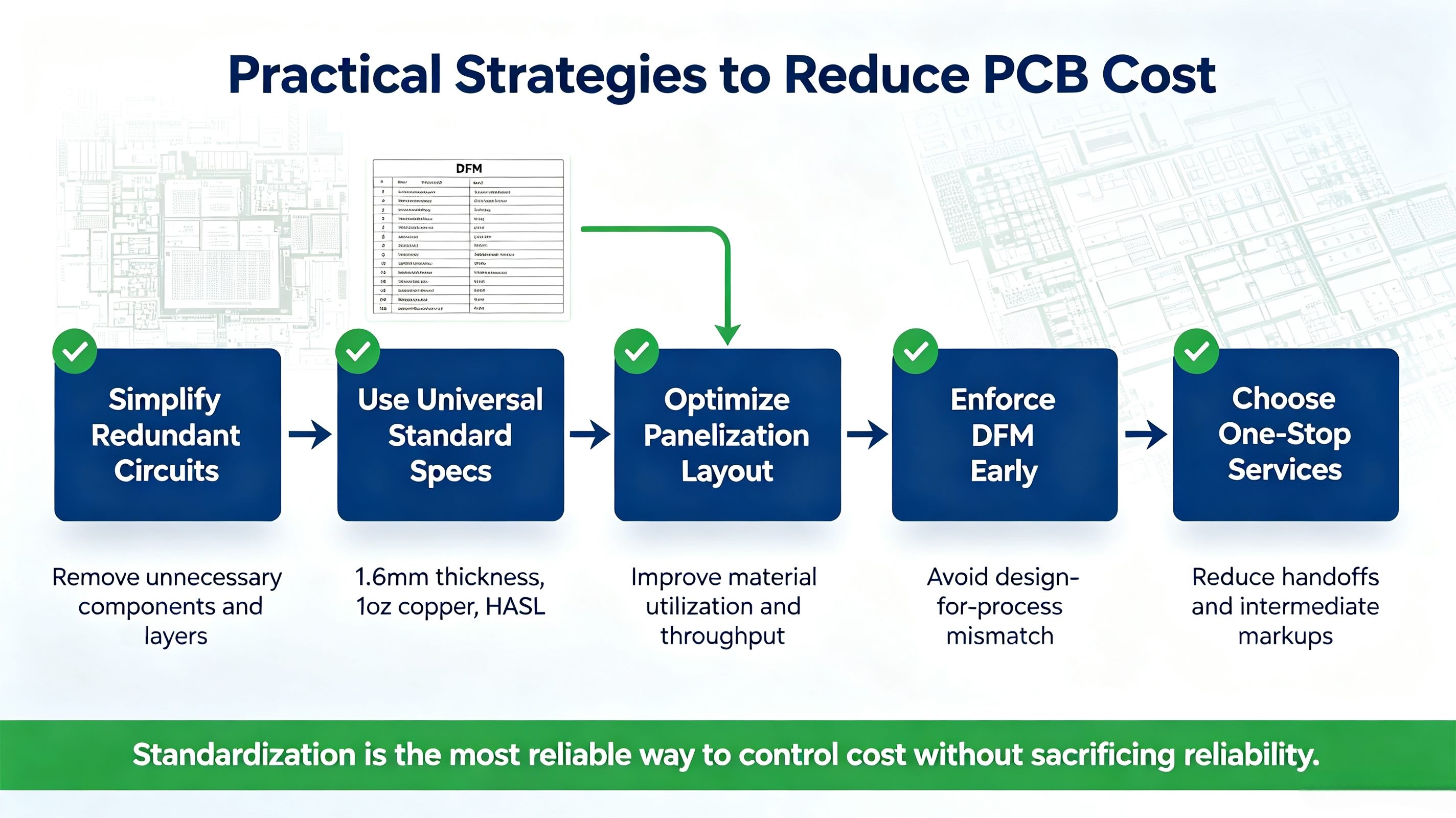
1. Simplify Circuit Design and Reduce Redundant Configuration
On the premise of meeting functional requirements, simplify redundant circuit modules, reduce unnecessary components and high-precision processes, and reasonably reduce board layer count. Kinji’s professional technical team provides free design optimization suggestions, helping customers balance functional performance and manufacturing cost.
2. Prioritize Universal Standard Specifications
Adopt industry-standard 1.6mm board thickness, 1oz copper weight, conventional trace and via parameters to avoid special process surcharges. For ordinary prototypes and mass-produced products, select HASL surface finish to replace high-cost ENIG, which can reduce surface processing cost by 30%–50% while meeting usage requirements.
3. Optimize Board Size and Panelization Layout
Try to adopt conventional rectangular outlines and mainstream standard dimensions to adapt to automated panel production. Kinji Group’s intelligent panelization system can automatically optimize board layout, maximize material utilization rate, and reduce unit cost through batch scale effect.
4. Strictly Implement DFM Manufacturability Standards
Align design specifications with mature industrial manufacturing process standards in the early design stage, avoid ultra-fine precision parameters and non-standard structures that require customized processing, and eliminate additional fees caused by design and process mismatch.
5. Adopt One-Stop Full-Cycle Service
Choose integrated PCB services covering design review, prototyping, mass production and assembly. The independent full-industry-chain production mode eliminates intermediate outsourcing markups, realizes seamless connection of all processes, and reduces comprehensive time cost and cooperation risk.

Conclusion
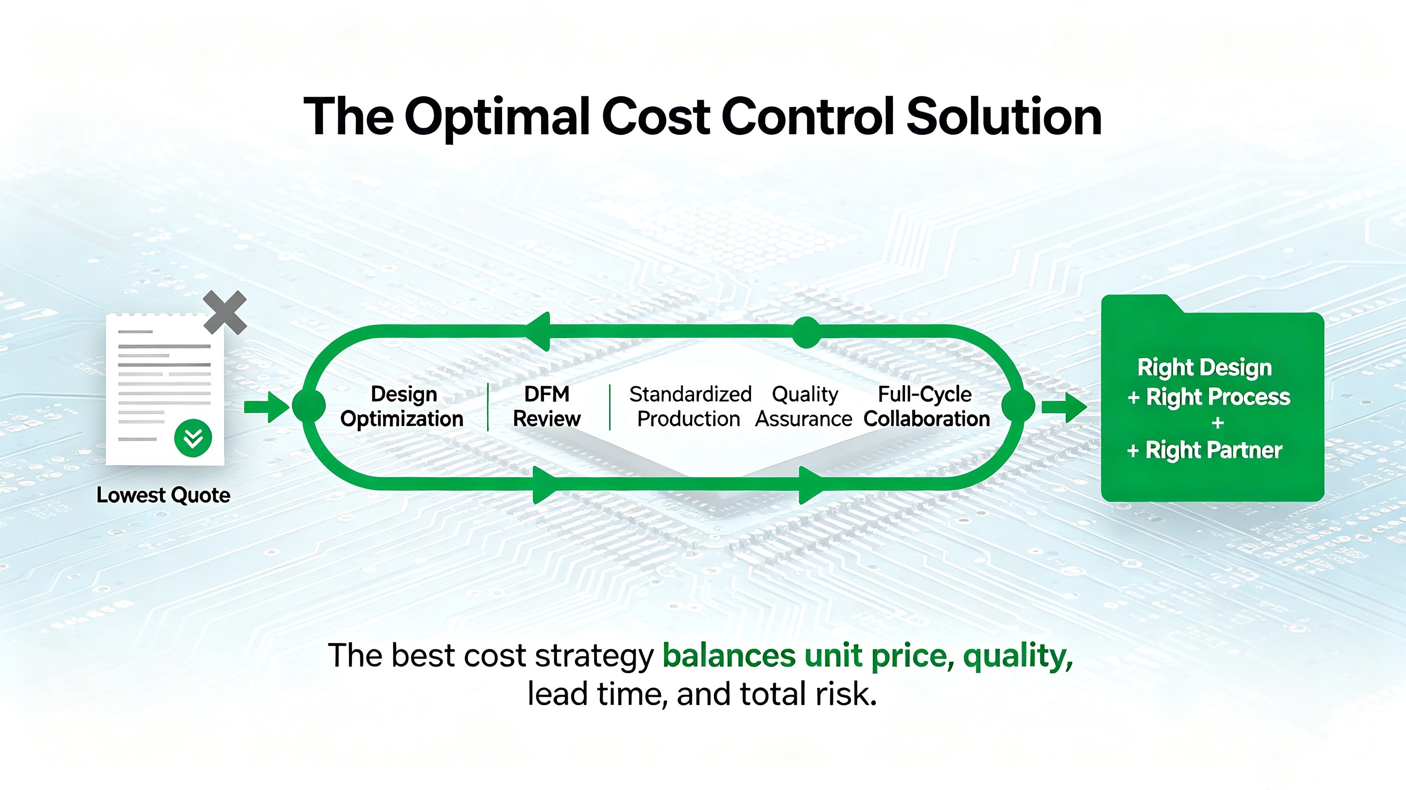
The comprehensive cost of custom PCBs is determined by design parameters, material selection, process difficulty, production mode and hidden cycle costs. Blind pursuit of high configuration and personalized design will lead to unnecessary budget waste, while excessive cost compression will affect product stability and yield. The optimal cost control solution is to formulate targeted design and production schemes according to product application scenarios, rely on standardized industrial processes, and cooperate with professional manufacturers with full-process capabilities.
With 29 years of PCB manufacturing accumulation, Kinji Group relies on intelligent production systems, independent process R&D capabilities and one-stop integrated services to help customers accurately control every cost link in custom PCB projects. From early design optimization and DFM review to mid-term standardized production and later quality assurance, we eliminate hidden expenditures while ensuring high-quality and high-reliability product output, helping all types of electronic projects achieve cost reduction, efficiency improvement and quality upgrade.
trending news
Contact Us