





Sorry, no sales person is available right now to take your call. Pls leave a message and we will reply to you via email as soon as possible.
Modular PCB Design: Reconstructing R&D Systems for Complex Electronic Projects with Engineering Thinking
2026-09-01
Modular PCB design is not merely a design technique but a core engineering mindset tailored for the R&D of medium-to-large-scale electronic projects. As component density escalates, BGA pin counts surpass critical thresholds, and signal rates enter the high-speed domain, the limitations of traditional integrated single-board design become pronounced—loss of design complexity control, soaring debugging difficulties, and skyrocketing maintenance costs emerge as critical bottlenecks in high-end electronic project development.
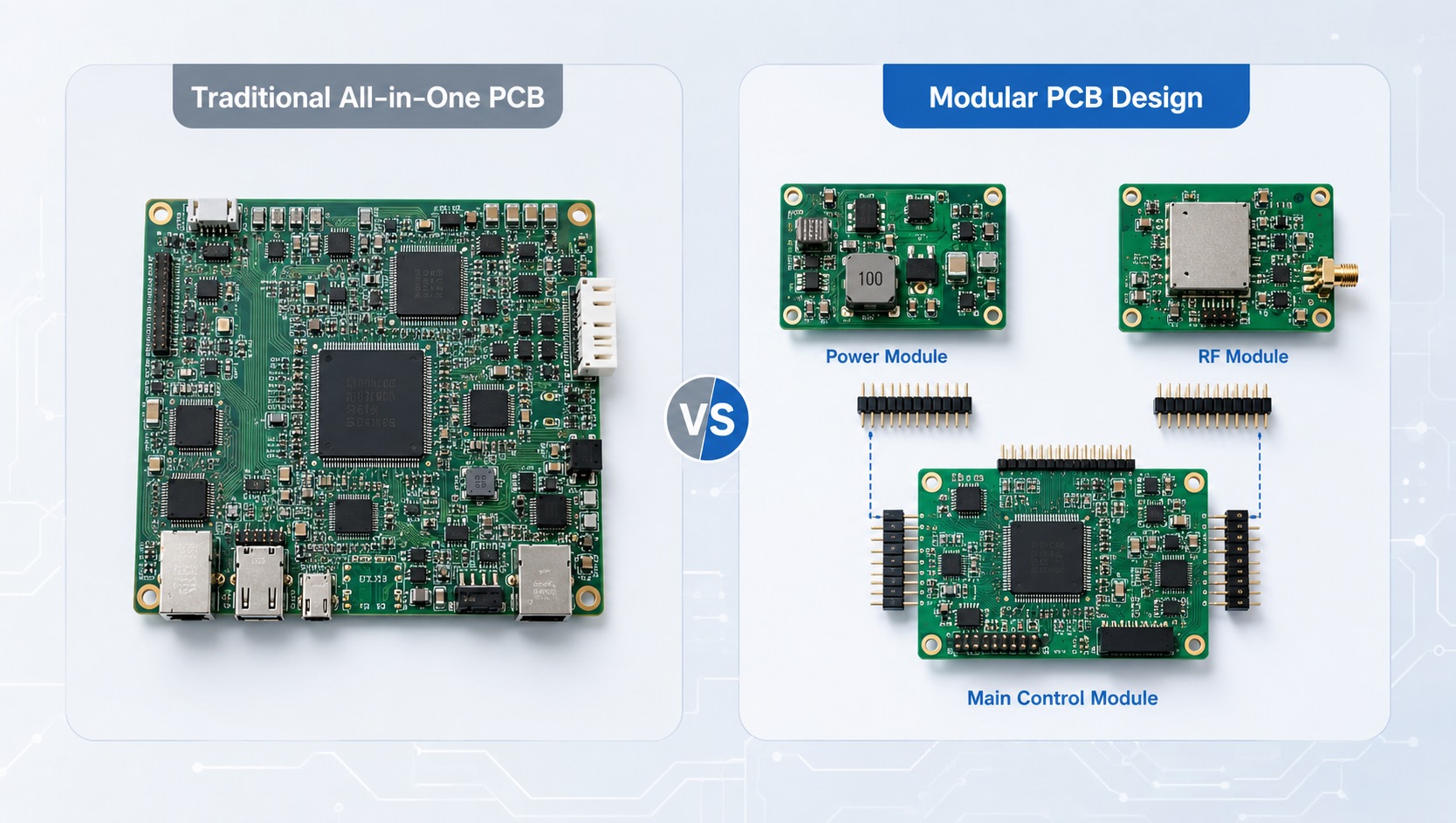
The core logic of modular PCB design lies in the standardized decomposition of complex electronic systems, breaking down and restructuring the overall system into a set of independent functional units. Each module adheres to the principles of "dedicated functionality and optimized performance," enabling precise partitioning of functions such as power supply, main control processing, RF transceiving, and signal conditioning. All functional units can independently undergo circuit design, performance tuning, and parameter optimization, and are ultimately integrated into a complete system via standardized interfaces. This design approach fundamentally simplifies the logic of complex system design, substantially enhancing project iterability, maintainability, and scalability, while aligning with the demands of industrialized, large-scale R&D and production.
Precisely Defining the Design Paradigm: On-Demand Selection Between Integrated and Modular Design
Integrated single-board design has its own applicable scenarios and should not be entirely dismissed. For simple, single-function circuit projects such as LED drivers and basic breakout boards, the integrated design workflow is straightforward and efficient, requiring no redundant engineering decomposition.
However, for complex projects involving mixed-signal systems, multi-voltage domain circuits, high-speed/high-frequency interfaces, and multi-device coordination, as well as team-based projects requiring parallel development by multiple engineers, modular design offers irreplaceable advantages. Its core value lies in fault isolation and localized change implementation, enabling precise issue localization and correction. When a single functional module experiences circuit anomalies, performance deviations, or compatibility issues, only the corresponding module needs optimization, repair, or replacement, eliminating the need for full-board redesign and rework. This transforms the traditionally inefficient model of global troubleshooting and full rework into a highly efficient model of targeted debugging and localized iteration, drastically compressing R&D and rework timelines.
Core of Modular Design: Standardized Interface Definition Determines System Reliability
The competitive edge of modular PCB design resides not in the internal circuit complexity of individual modules, but in the standardized and规范化 design of module boundaries and interconnecting interfaces. A high-quality functional module must feature clear external electrical definitions, specifying signal I/O types, supply voltage parameters, communication protocol standards, and loop design rules, thereby ensuring system stability at the foundational level after multi-module integration.
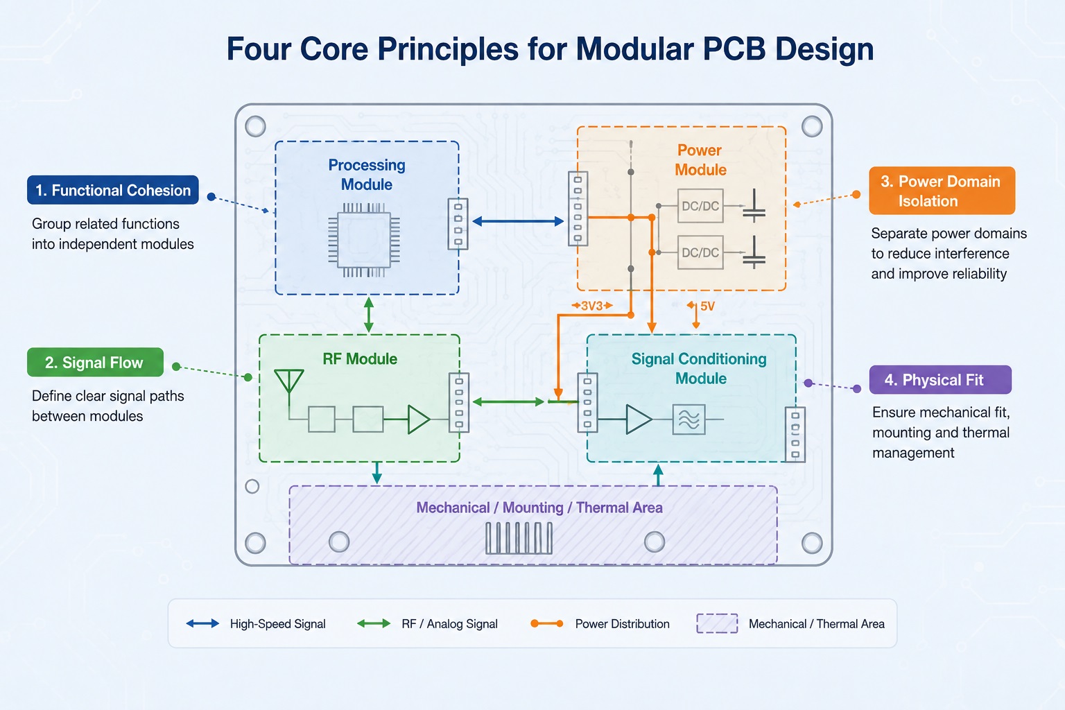
In practical engineering design, module boundaries can be scientifically delineated along four core dimensions to avoid circuit coupling interference and design redundancy:
First, the principle of functional cohesion. Concentrate components that realize the same core function within a single module, ensuring functional independence and eliminating cross-module circuit coupling and function overlap, so that each module has clear responsibilities and dedicated functionality.
Second, the principle of signal flow. Strictly partition modules along signal transmission chains, aligning with the complete logic of signal input, processing, and output, to prevent signals from traversing modules repeatedly, thereby reducing signal attenuation and crosstalk risks.
Third, the principle of power domain isolation. Divide modules according to voltage levels and power supply requirements, placing circuits with different voltages and power consumptions in separate zones. This facilitates fine-grained management of the overall power system and effectively suppresses electromagnetic noise interference between high-voltage and low-voltage circuits.
Fourth, the principle of physical adaptation. Incorporate mechanical constraints such as structural enclosures, mounting holes, and heat dissipation areas into the module physical layout planning, balancing electrical performance with structural assembly and thermal performance compatibility.
Meanwhile, interface design should adhere to standardization and uniformity principles, employing standard interconnect structures such as common pin headers and receptacles, and unifying naming conventions for signal, power, clock, and other ports. This ensures module universality, reusability, and compatibility, laying the groundwork for product iteration, module replacement, and volume production.

Throughout the Entire Process: Modular Design Must Align with Manufacturing Standards
At present, most R&D teams can achieve modular decomposition at the design stage, but often overlook optimization for manufacturing, resulting in high-quality designs failing to translate into high-yield, high-reliability volume products. The modular PCB structure imposes far stricter requirements on process technologies, panelization schemes, SMT placement procedures, and depaneling techniques than traditional single-board designs. Any deviation in any process step can compromise overall product quality.
To avoid disconnects between design and production, five major process risks must be proactively addressed:
1. Insufficient panel spacing – Inadequate clearance for V-cut and stamp-hole routing can lead to circuit trace damage and substrate cracking during depaneling.
2. Missing fiducial markers – Insufficient optical fiducial marks in multi-module panel designs can cause SMT placement misalignment, affecting soldering accuracy.
3. Incomplete engineering documentation – Inconsistent or missing Gerber files, drill files, BOM lists, and pick-and-place coordinate files cause production communication errors.
4. Missing electrical parameter specifications – Failure to clearly specify critical requirements such as high-speed signal impedance control and differential pair routing compromises high-speed signal integrity.
5. Panel utilization and economics not aligned with the manufacturer – Neglecting to optimize material utilization and panel economy in multi-module panels during the design phase can directly erode per-board cost control—a point particularly critical in the "deep dive into volume production" stage.
Deepening Volume Production: Professional Manufacturing Partners Are the Cornerstone of Modular Projects
The full value of modular PCB design ultimately materializes through standardized, refined production and manufacturing. The process complexity and quality control challenges of complex multi-module circuit boards far exceed those of ordinary single boards. Front-end design optimization alone cannot guarantee product stability in mass production. Selecting a manufacturing partner with proven experience in modular board production is the key to successful project realization.
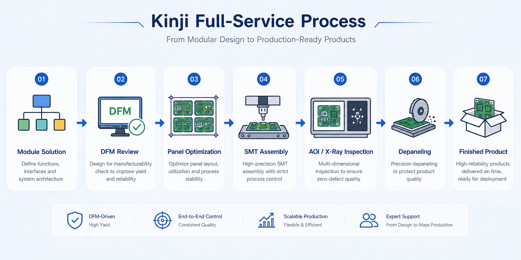
A professional PCB manufacturing partner can conduct a pre-production DFM (Design for Manufacturability) review, offering optimization recommendations for process bottlenecks such as trace width/spacing, annular ring dimensions, and routing density before panelization, thereby preemptively addressing design flaws. For special structures involving mixed multi-module panelization, differentiated routing, and coexistence of high-speed and low-speed circuits, the partner can coordinate process standards across modules, balancing performance requirements with production feasibility. Moreover, leveraging mature SMT flexible capacity, standardized material supply systems, and comprehensive quality inspection processes—including AOI, X-Ray inspection, and electrical performance testing—ensures that each functional module independently meets specifications and the overall system performs reliably.
Kinji Group: Full-Process Enabler for Modular PCB Design Volume Production
With years of deep expertise in PCB manufacturing and SMT assembly, Kinji Group focuses on multi-variety, medium-to-large-volume, high-complexity circuit board production, accumulating extensive experience in the implementation and mass production of modular PCB structures. The company goes beyond standard circuit board fabrication, striving to bridge the technical gap between design and manufacturing, fully preserving the core advantages of modular design while providing customers with end-to-end solutions from DFM review to production delivery.

Core service capabilities span four dimensions:
· Proactive DFM review services – Comprehensive manufacturability verification is conducted prior to panelization, with customized panelization schemes tailored to multi-module structures, defining process windows and optimizing design risks upfront.
· Flexible panel layout solutions – Supports both same-module repetition and mixed-module panelization, with optimized V-cut and stamp-hole layouts to reduce depaneling damage and improve production yield.
· End-to-end quality control system – Covers the entire chain from incoming material inspection, SMT precision placement, reflow soldering, AOI, X-Ray inspection, to electrical functional testing, enabling independent verification of individual modules and full-board performance validation.
· Meticulous project version management – Adapts to the high-frequency iteration demands of modular projects, establishing standardized engineering communication and version control mechanisms to ensure efficient project coordination and traceable change management.
Conclusion: Modularity Is a Technical Methodology and a Long-Term Product Strategy
Modular PCB design is a core engineering methodology suited to the evolution of the modern electronics industry, and more importantly, a strategic product approach that supports long-term product iteration, efficient team collaboration, and stable quality control. Through systematic module decomposition, standardized interface definition, and full-process process alignment, it effectively addresses industry pain points such as design complexity, prolonged debugging cycles, high iteration costs, and maintenance difficulties.
The complete realization of modular design value demands deep collaboration between front-end design and back-end manufacturing. Choosing a manufacturing partner with proven experience in modular board production is not the endpoint of design but the starting point for delivering design value. In the face of ever-increasing product complexity and accelerating iteration cycles, empowering R&D with modular engineering thinking and complementing it with professional full-process manufacturing services effectively reduces project risks and enhances product competitiveness.
Kinji Group is dedicated to full-process PCB services, leveraging its professional process capabilities to undertake a wide range of complex modular PCB projects. We help enterprises standardize, streamline, and scale their complex R&D projects, making high-end electronic development more controllable and more reliable.
trending news
Contact Us