





Sorry, no sales person is available right now to take your call. Pls leave a message and we will reply to you via email as soon as possible.
Latent Microvia Failures in HDI PCBs: Root Causes and Reliability Solutions
2026-08-25
The Underrated Crisis in High-Density Interconnect Production & Testing
High-Density Interconnect (HDI) PCBs serve as the core hardware foundation for today’s high-end electronics, empowering 5G infrastructure, AI high-speed computing, precision automotive electronics, and ultra-compact optical module devices. Despite mature fabrication workflows, HDI boards remain one of the most challenging product categories in terms of consistent yield and long-term reliability. Subtle, non-visible defects frequently emerge during testing or mass production, causing unplanned rework, delayed product launches, elevated manufacturing costs, and latent safety risks for mission-critical equipment.
Industry Wide IPC Consensus: Latent Microvia Failure Is a Systematic Industry Risk
The IPC has formally identified hidden microvia reliability issues as a critical industry challenge affecting high-performance HDI products. A well-documented industry phenomenon reveals that certain microvia failures are triggered during high-temperature reflow processes yet remain undetectable under standard room-temperature testing conditions. These latent defects tend to surface in later assembly stages or after end-product deployment, resulting in exponentially higher rework costs and posing potential operational and safety hazards for high-reliability applications.
Three Core Root Causes of HDI Latent Failure Modes
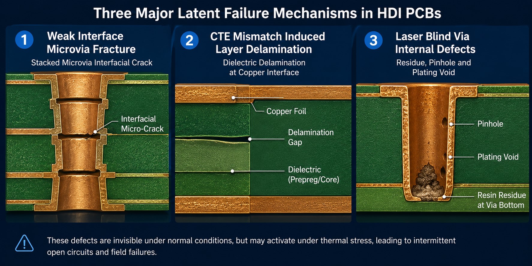
1. Weak Interface Microvia Fracture (Most Elusive Defect)
The most difficult failure to screen is microvia interfacial cracking occurring at the metallurgical boundary between microvias and inner copper layers. Under thermal stress during reflow, tiny fractures form at the bonding interface; once the board cools to room temperature, the cracks close and recover conductivity, allowing the board to pass standard electrical tests. Complex stacked microvia structures, especially multi-layer stacked configurations, are far more susceptible to this intermittent failure mode, which leads to unstable signal transmission or sudden open circuits in field operation.
2. Thermal Stress Delamination from CTE Mismatch
HDI laminates consist of epoxy resin, glass fiber, and copper foil with inconsistent coefficients of thermal expansion (CTE). During lead-free reflow cycling with peak temperatures up to 260°C, repeated thermal expansion and contraction generate persistent interfacial shear stress. When accumulated stress exceeds the material’s interfacial bonding strength, micro-cracks initiate and gradually develop into layer delamination, causing impedance drift, intermittent disconnection, and long-term structural instability.
3. Laser Blind Via Bottom Defects
Laser blind vias enable ultra-fine circuit miniaturization but introduce unique reliability vulnerabilities. Key failure triggers include carbonized resin residues generated during laser ablation, which form insulating barriers and degrade electrical conductivity; micro pinholes in electroless copper layers that reduce effective interfacial bonding; and trapped electroplating bubbles caused by improper pulse frequency or excessive aspect ratios (AR > 0.8), resulting in inner voids and weakened via structural integrity.
Why Conventional Testing Methods Fail to Capture Latent Risks
AOI Inspection Limitations
Standard Automated Optical Inspection (AOI) effectively identifies surface defects such as solder bridging, missing solder, and component misalignment. However, AOI cannot penetrate BGA/QFN packaging or capture inner-layer micro-cracks, interfacial delamination, and subsurface voids — all of which only activate under thermal cycling stress.
The Fundamental Challenge of Room-Temperature Testing
The biggest pain point in HDI quality control is latent defect self-recovery. Thermally induced microvia fractures physically close at room temperature, enabling boards to pass standard continuity and resistance tests while hiding critical structural weaknesses. This leads to “test-pass but field-fail” scenarios that severely impact product consistency and equipment reliability.
Advanced Testing & Reliability Optimization Solutions
Four-Wire Precision Low-Resistance Testing
Milliohm-level four-wire resistance monitoring accurately captures subtle resistance fluctuations during thermal cycling, enabling early detection of microvia fatigue and interfacial degradation before complete open-circuit failure occurs.
IPC Standard Thermal Stress Qualification (IPC-TM-650 2.6.27A)
Compliant with official IPC high-reliability specifications, this protocol requires test coupons to complete six full reflow thermal profiles with real-time four-wire resistance tracking. A maximum resistance increase of 5% is allowed throughout the entire thermal cycle, providing authoritative screening for latent microvia defects that standard testing cannot identify.
High-Precision FIB-SEM Microsection Analysis
Focused Ion Beam (FIB) cross-sectioning enables damage-free, nanoscale microscopic observation of microvia interiors, precisely verifying crack morphology, void distribution, and interfacial delamination mechanisms to support root-cause analysis and process optimization.
Industry Best Practices for Stable HDI Yield & Reliability
Material Selection Standards
Adopt high-Tg substrates (Tg > 170°C) with low thermal expansion (CTE < 3.5 ppm/°C) and low-roughness HVLP/RTF copper foil (Rz ≤ 5μm) to minimize thermal stress and enhance interfacial adhesion stability for high-frequency, high-density circuits.
Strict Process Control
Maintain post-desmear bottom copper ≥ 6μm before electroplating; stabilize electroplating solution parameters and equipment operation consistency to eliminate voids, pinholes, and uneven copper deposition inside microvias.
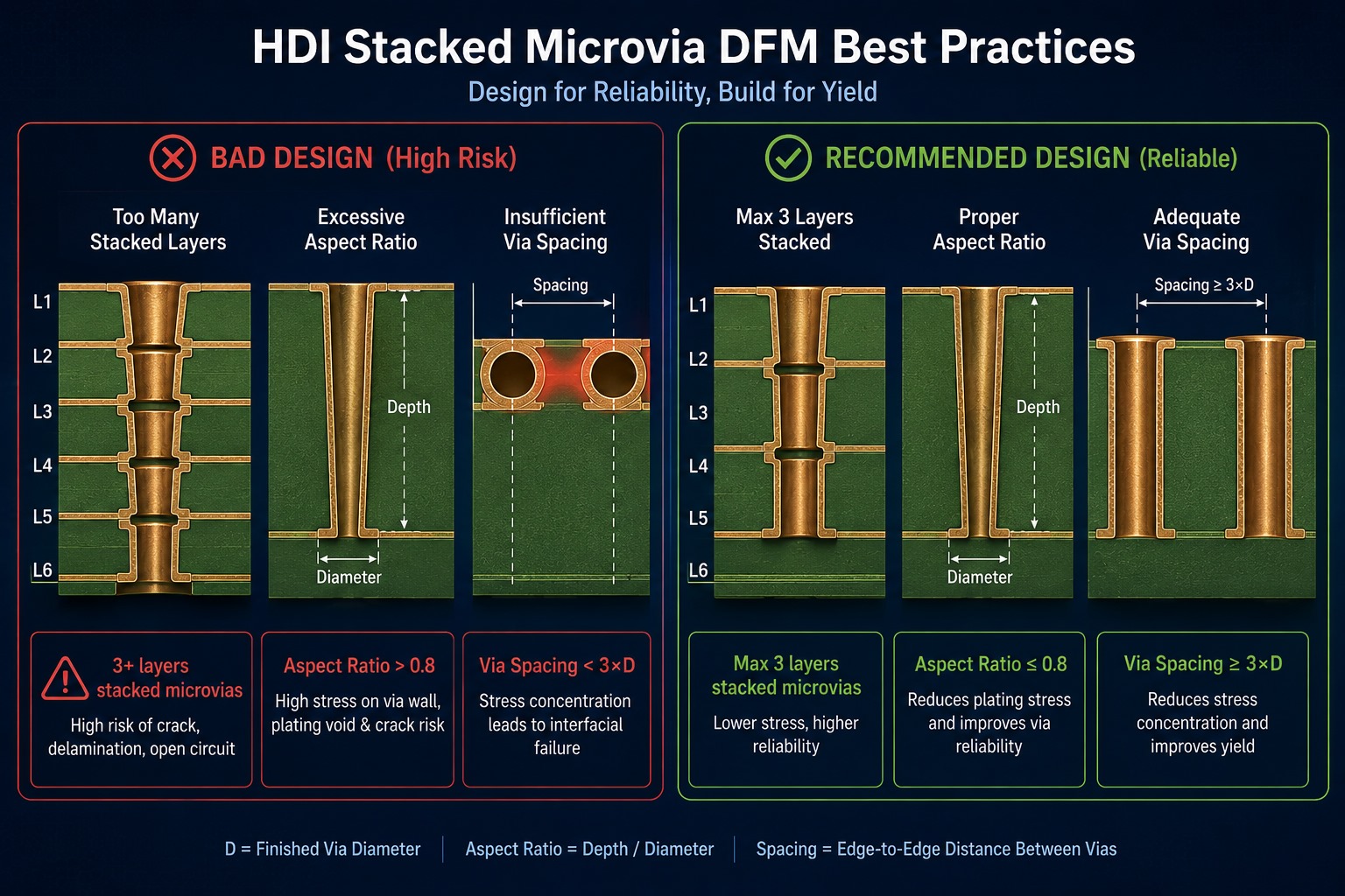
DFM Design Optimization
Control blind via diameter ≤ 150μm and aspect ratio ≤ 0.8; limit stacked microvia layers to maximum 3 stacks; set adjacent via spacing to no less than three times the via diameter to avoid concentrated thermal stress and structural fatigue.
Multi-Dimensional Testing Mechanism
Implement a combined quality control system integrating AOI visual inspection, X-ray internal scanning, IPC-standard thermal stress testing, and four-wire resistance monitoring. Random microsection sampling and microscopic review ensure continuous process iteration and long-term batch stability.
Conclusion
HDI reliability challenges stem not from visible surface defects, but from hidden thermal-induced structural failures inside microvias and dielectric layers. Systematic reliability risks including weak interfacial bonding, CTE thermal mismatch, and laser via structural defects persist as core pain points for high-end HDI manufacturing.
By adopting high-stability material specifications, standardized DFM constraints, rigorous thermal stress qualification, and multi-level precision testing systems, manufacturers can effectively eliminate latent HDI failures, stabilize mass-production yield, and deliver consistent, high-reliability PCBs for AI computing, 5G communication, medical devices, and high-precision industrial equipment.
Backed by mature HDI process control and full-range reliability validation capabilities, Kinji Group helps customers mitigate latent microvia risks from DFM review through prototype and mass-production phases.
Reach out to our engineering team for technical consultation on your high-density PCB projects.
trending news
Contact Us