





Sorry, no sales person is available right now to take your call. Pls leave a message and we will reply to you via email as soon as possible.
Back-Drilling for PCB: Technical Principles, Application Scenarios and Design Specifications
2026-08-20
1. Process Definition and Core Value
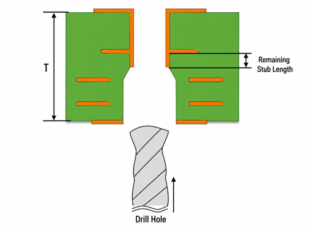
Back-drilling is a high-precision special process in PCB manufacturing. Its core principle is to remove unwanted conductive copper stubs inside vias by means of controlled-depth drilling. It addresses signal reflection, loss and interference in high-speed / high-frequency transmission, guarantees signal integrity (SI) and system stability, and serves as one of the critical processes for high-performance interconnection on premium-grade PCBs.

2. Key Application Scenarios and Design Requirements
| Application Field | Typical Products | Key Signal Characteristics | Core Objectives of Back-drilling |
| High-speed Digital Communications | Routers, switches AI servers, data-center equipment | Multi-Gbps high-speed differential signals, often 10 Gbps and above | Shorten stub length, suppress signal reflection and jitter Meet eye-diagram specifications and ensure reliable high-speed data transmission |
| High-frequency RF & Wireless | Base-station antennas, power amplifiers (PA)Radar, RF modules | High-frequency analog signals, ranging from several GHz to tens of GHz | Reduce parasitic capacitance and inductance introduced by stubs, suppress resonance Minimize signal distortion and insertion loss |
| High-speed Computing & Storage | CPU/GPU mainboards,memory modules (DDR5/DDR6),AI accelerator cards | Extremely high data-rate, strict timing control and impedance-matching requirements | Optimize via impedance continuity, reduce deterministic jitter (DJ) and random jitter (RJ) Improve stability of computing and storage systems |
| Special-purpose Scenarios | Optical-module PCBs,special interconnection boards | Special interconnection requirements, partially for high speed signals | Cut temporary conductive traces to realize special structural interconnection Further optimize overall signal-transmission performance |
3. Criteria for Deciding Whether Back-drilling Is Required
The necessity for back-drilling mainly depends on signal rate and the electrical-length impact of stubs on signal integrity.
1. Quantitative Engineering Criterion Back-drilling shall be adopted when the electrical length of a via stub exceeds 1/10 of the equivalent electrical length of the signal rising edge. In practical engineering, this condition generally corresponds to signal rates ≥ 1 Gbps. For signals at 1 Gbps or higher, the influence of stubs must be evaluated and a back-drilling scheme planned.
2. Validation by Simulation The most reliable method is system-level interconnect simulation (tools such as Ansys, Cadence). Modeling quantifies how stub length and impedance affect reflection, loss and jitter, and accurately determines whether back-drilling is needed and the required drilling depth.

4. Core Process Flow and Technical Considerations
4.1 Standard Process Flow
Back-drilling is coordinated with regular PCB manufacturing: Primary drilling → via metallization (electroless copper deposition & electroplating) → controlled-depth back-drilling from the rear side (stopping at safe offset above target layer) → cleaning (drill-swarf removal) → quality inspection.
4.2 Key Technical Points
Precision Depth Control: High-precision CNC drilling machines (e.g. Schmoll from Germany, Hitachi from Japan) adopt Z-axis closed-loop control, optical alignment and real-time board-thickness compensation to achieve micron-level depth accuracy. To avoid damaging target-layer pads, a safety margin of 8-10 mil (0.2-0.25 mm) is reserved above target pads, with depth tolerance controlled within ±5-10 mil.
Drill-bit Size Selection: The back-drill bit shall be 8-10 mil (0.2-0.25 mm) larger in diameter than the original via hole. This fully removes residual copper on via-sidewalls and prevents leftover conductive segments from degrading signal performance.
Process Combination Optimization: Back-drilled cavities are commonly filled with high-temperature-resistant, low-expansion special resin via resin-plugging. This keeps contaminants out in downstream processes, maintains board flatness and facilitates subsequent lamination and solder-mask application.
Quality Inspection: Traditional metallographic cross-sectioning is destructive and low-efficiency. Advanced non-destructive testing uses dedicated test vias and test circuits. Continuity or impedance measurement quickly verifies stub qualification and boosts inspection efficiency by over 80%.
4.3 Design-to-Manufacturing Collaboration
Back-drilling increases PCB cost by approximately 10%-20% and extends lead-time by 1-2 working days. Close early-stage collaboration between design and manufacturer is essential:
- Clear specification: Mark networks for back-drilling, target start-stop layers, target residual stub length (recommended ≤ 8 mil) and tolerances in Gerber files and fabrication notes.
- Verify manufacturer capability: Confirm achievable depth tolerance (typical ±5-10 mil; high-end down to ±3 mil), minimum annular-ring capability (recommended ≥ 8 mil), and resin-plugging compatibility.
- Design-side optimization: Minimize unused penetrated layers for high-speed-signal vias to inherently shorten stubs. Avoid placing back-drilled vias in dense-pad regions to reduce alignment difficulty and pad-damage risk.
5. Future Development Trends
Driven by rising performance demands from AI, 5G and high-speed computing, back-drilling evolves toward higher precision, intelligence and multi-process integration.
- Higher Precision: New technologies including 3D inner-layer-aware one-shot back-drilling and thickness-memory compensation improve stub-length control by over 40%. Stub lengths within 5 mil are achievable for premium-grade applications, supporting signal rates of 56 Gbps and beyond.
- Intelligent & Automatic Manufacturing: AI-enhanced CAM software auto identifies high-speed-signal nets, selects vias for back-drilling and optimizes tool paths. CCD vision positioning combined with laser ranging delivers micron-level alignment accuracy and reduces human-introduced errors.
- Multi-process Integration: In high-end HDI and any-layer-interconnect PCBs, back-drilling complements blind-via, buried-via and laser-microvia technologies. Combined “blind-buried-via plus back-drilling” solutions realize high-density, high performance and miniaturized PCB designs.
Back-drilling demands strict equipment capability and DFM collaboration. Kinji Group delivers high-precision back-drilling together with resin plugging for high-speed multi-layer and HDI PCBs. We offer pre-production DFM review, prototype validation and mass-production support. Feel free to share your stack-up and Gerber files for free technical assessment and quotation.
trending news
Contact Us