





Sorry, no sales person is available right now to take your call. Pls leave a message and we will reply to you via email as soon as possible.
Kinji 6-Layer Buried Copper Block PCB: Benchmark Solution for Thermal Management and Current-Carrying Capacity in High-Power Scenarios
2026-08-11
In high-power-density applications such as new energy vehicles, industrial IGBTs, and high-performance computing servers, a PCB's thermal management capability, current-carrying capacity, and long-term reliability directly determine system stability and service life. Kinji introduces its 6-layer buried copper block PCB, integrating an embedded copper process, advanced HDI architecture, and high-stability substrate materials. This solution delivers a comprehensive framework combining efficient heat dissipation, high-current handling, and reliable interconnections—providing a solid hardware foundation for power electronics operating under demanding conditions.
Core Process & Parameters: Technical Architecture Tailored for High-Power Scenarios
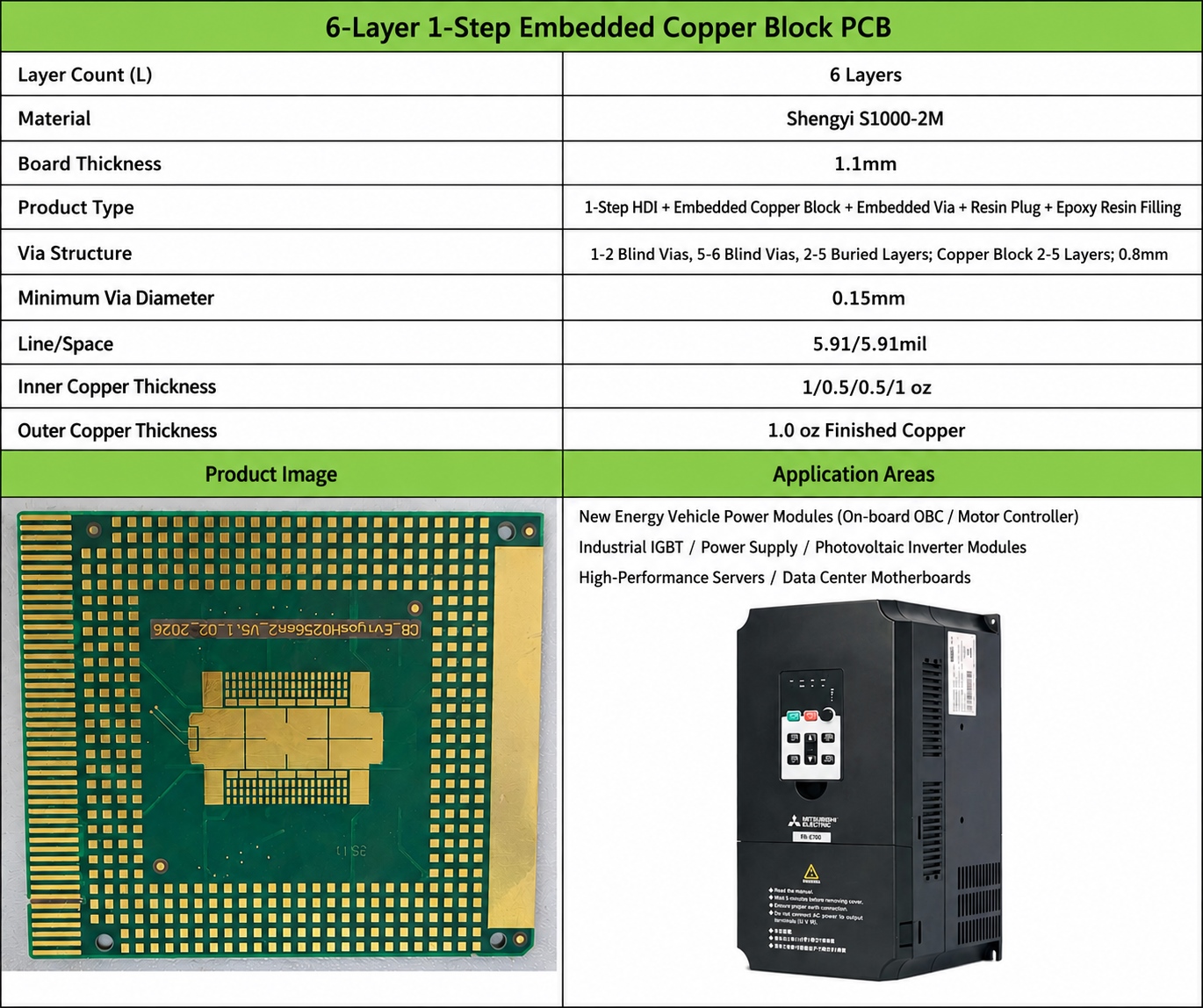
Every parameter of this PCB is engineered around three core requirements—high power, high heat dissipation, and high reliability—achieving a deep integration of process and performance.

Key Technological Breakthrough: Buried Copper Block Process Addresses High-Power PCB Challenges
Conventional PCBs in high-power-density environments face three major obstacles: thermal runaway risks due to high thermal resistance, current-carrying bottlenecks caused by the skin effect, and reliability failures induced by CTE (Coefficient of Thermal Expansion) mismatch. Kinji systematically overcomes these challenges through fundamental architectural innovation with its buried copper block technology.
1. Vertical Thermal Conduction Architecture – Breaking Through Local Heat Flux Density Bottlenecks
Traditional via-based heat dissipation solutions achieve vertical thermal conductivity of only 10–20 W/(m·K), which falls short when power devices (e.g., IGBTs, MOSFETs) generate local heat flux densities exceeding 100 W/cm². Kinji's integrated buried copper block process builds highly thermally conductive copper pillars (≈400 W/(m·K)) within the PCB, enabling direct heat transfer from the heat source layer to multilayer heat-spreading copper foils. This reduces vertical thermal resistance by over 40%, effectively controlling hotspot temperatures beneath devices within safe operating ranges and completely eliminating thermal runaway and thermal fatigue failure risks.
2. Low-Impedance Current-Carrying Paths – Suppressing Skin Effect and Joule Heating Losses
Addressing the insufficient effective conductive cross-section caused by the skin effect in high-frequency, high-power loops, the buried copper block provides a significantly lower-impedance current path capable of sustaining continuous currents at the hundred-ampere level. Combined with 1 oz outer-layer copper foil, this design substantially reduces skin-effect losses in AC circuits. Compared with pure copper foil routing, the buried copper block lowers loop DC resistance by over 60%, markedly reducing Joule heating and improving power module conversion efficiency.
3. Embedded Integrated Design – Optimizing System Power Density
The buried copper block is embedded between layers and integrally formed with the PCB substrate, requiring no additional board space and not affecting surface component placement or BGA fan-out routing. Without compromising thermal performance, this design eliminates redundant structures such as external heat sinks and thermal pads used in conventional approaches, facilitating device miniaturization and weight reduction—particularly advantageous for space-constrained applications like new energy vehicle controllers and industrial frequency converters.
4. CTE Matching Optimization – Enhancing Long-Term Reliability Under Thermal Cycling
The buried copper block achieves a precisely matched CTE with the Shengyi S1000-2M substrate, effectively alleviating shear stress caused by CTE mismatch during thermal cycling and avoiding common failure modes such as wall cracks, delamination, and copper foil peeling. Coupled with 1-step HDI buried/blind vias and resin plugging, the process further eliminates residual voids in blind vias and plating voids, ensuring insulation reliability and mechanical stability under high-voltage, high-load conditions.
Diverse Scenario Adaptability: Proven Applications Across Three High-Power Sectors
With customized process design and stringent quality control, Kinji buried copper block PCBs have achieved volume production across multiple high-reliability industry segments. The solutions precisely address real customer pain points with quantifiable, traceable results, earning high recognition from industry leaders.
New Energy Vehicle Power Module (On-Board OBC Charger)
Client & Scenario: A leading domestic new energy vehicle manufacturer's pure electric SUV on-board OBC charger project, requiring 22 kW high-power fast charging within a compact space (≤280 mm × 180 mm × 60 mm), compliance with automotive-grade -40°C to 125°C thermal cycling standards, and device junction temperatures maintained below 150°C.
Original Challenge: The customer's conventional aluminum-based PCB + heat sink solution saw power MOSFET (IPB65R110CFD) junction temperatures reach 178°C during fast charging—far exceeding the safety threshold—frequently triggering overtemperature protection and interrupting charging. The 12 mm-thick heat sink also consumed excessive space, failing to meet compactness requirements.
Solution & Results: Adopting Kinji's 6-layer buried copper block PCB, a 0.8 mm copper block was custom-embedded beneath the MOSFET heat source to establish a vertical heat conduction channel, reducing the fast-charge junction temperature from 178°C to 153°C—fully compliant with automotive safety standards and eliminating charging interruptions. The 12 mm heat sink was removed, leaving only a 3 mm thin thermal pad, reducing overall PCB thickness from 8.2 mm to 5.7 mm and board volume by 30%, perfectly fitting the vehicle's confined space. This solution has entered volume production with over 120,000 units delivered, surviving 1,000 automotive-grade thermal cycles (-40°C to 125°C, 1 hour/cycle) with no delamination, wall cracks, or copper peeling. Yield consistently exceeds 99.8%, helping the customer's vehicle model successfully pass new energy vehicle certification.
Industrial Power Electronics (11 kW Motor Drive Module)
Client & Scenario: A leading domestic industrial frequency converter manufacturer. Its 11 kW motor drive module, used in mining machinery and assembly line equipment, must operate continuously under dust, high ambient temperatures (up to 65°C), and high-frequency vibration (10–50 Hz). Requirements include IGBT (FF300R12KT4) long-term operating temperature ≤120°C and equipment MTBF ≥20,000 hours.
Original Challenge: The conventional 6-layer PCB without buried copper design resulted in IGBT local hotspot temperatures reaching 142°C and line voltage drops ≥0.8 V, leading to frequent failures including IGBT burnout and abnormal drive signals, with a failure rate of 8.3%—severely impacting reputation and after-sales costs.
Solution & Results: The Kinji buried copper block solution optimized copper block placement, embedding 0.8 mm blocks into layers 2–5 beneath the IGBT mounting area while optimizing copper thickness distribution to enhance current capacity. Hotspot temperatures dropped from 142°C to 115°C, safely below threshold, while line voltage drop fell below 0.5 V, reducing Joule losses and boosting motor drive module conversion efficiency from 94.2% to 96.7%. CTE matching and resin plugging processes significantly enhanced vibration resistance for mining machinery applications. After volume deployment, equipment failure rates fell to 1.7%, MTBF increased to 28,000 hours—far exceeding requirements—and the elimination of auxiliary cooling structures reduced per-unit costs by 8%, saving the customer over RMB 3 million annually in after-sales and manufacturing costs.
High-Performance Server / Data Center Motherboard (AI Server Power Supply Module)
Client & Scenario: A leading domestic data center solutions provider. Its AI server power supply modules, used for AI training and big-data analytics, must deliver stable power to CPUs (Intel Xeon Platinum 8470C) and GPUs (NVIDIA A100), supporting continuous 35 A currents, voltage fluctuation ≤±2%, module temperature ≤90°C, and high-density routing (≥120 lines/inch).
Original Challenge: The conventional PCB lacked sufficient current-carrying capacity, causing severe heating in power loops with operating temperatures reaching 98°C. Excessive voltage drops led to unstable CPU/GPU power delivery and performance throttling, while routing density failed to meet high-density interconnection needs.
Solution & Results: The Kinji 6-layer buried copper block PCB uses the copper block as the main low-impedance current path for the power loop, replacing conventional foil routing. This reduced loop DC resistance by 62%, lowered voltage drop to within 0.3 V, and stabilized voltage fluctuation at ≤±1.5%—ensuring stable CPU/GPU power delivery. The copper block rapidly extracts heat from the loop, keeping supply module temperatures steadily below 82°C and eliminating overheating and throttling issues. Combined with 1-step HDI buried/blind vias and precision routing (line width/spacing 5.91/5.91 mil), routing density reached 135 lines/inch, achieving efficient isolation between power and signal layers to prevent interference. This solution has been deployed across three large-scale data center projects with over 80,000 units delivered, supporting 7×24-hour continuous stable operation and improving computing output stability by 25%, with repeat orders received from the customer.
Kinji Technical Support: Full-Chain Assurance from Design to Volume Production
As a professional PCB manufacturer, Kinji offers not only mature buried copper block process solutions but also full-process service capabilities—from collaborative design and process validation to mass production:
· Supports customized copper block specifications, optimizing block size, embedded layer position, and layout based on customer heat-source distribution, power requirements, and mounting dimensions, with one-on-one DFMEA design analysis to proactively mitigate process risks.
· Full compliance with IPC-A-600, IPC-6012, and other international standards; equipped with professional cross-section analysis laboratories, thermal cycling test systems, and insulation withstand-voltage testing systems. Every board undergoes 100% visual inspection, sample thermal cycling, and cross-section verification to ensure performance consistency.
· For new energy, industrial, data center, and other high-reliability sectors, offers customizable test reports, process documentation, and RoHS, REACH, and other environmental compliance certificates to accelerate product certification and shorten project lead times.
Kinji buried copper block PCBs combine process innovation to solve thermal management and current-carrying challenges in high-power scenarios, with proven volume-production case studies validating performance. The solution delivers a balanced combination of performance, reliability, and cost-effectiveness. Whether in new energy vehicle power modules, industrial power equipment, or high-performance server cores, this PCB serves as the "invisible cornerstone" of stable system operation—empowering customers to seize performance leadership in the high-power era and solidify their competitive edge.
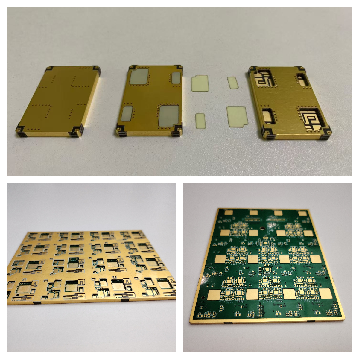
Kinji Buried Copper Block PCB Product Display

trending news
Contact Us