





Sorry, no sales person is available right now to take your call. Pls leave a message and we will reply to you via email as soon as possible.
Kinji High-Performance Sapphire Substrate: Defining a New Benchmark for High-End Electronic Device Quality
2026-08-05
Against the backdrop of the ongoing industry trend toward higher frequencies, miniaturization, greater reliability, and higher integration in high-end electronic devices, the dielectric performance, mechanical properties, surface flatness, thermal stability, and process compatibility of substrate materials have become critical bottlenecks determining core device performance and market competitiveness. As a specialized, high-precision PCB precision manufacturing platform recognized as a "Specialized and Sophisticated" enterprise, Kinji has long been deeply engaged in the field of high-end specialty boards, including specialty ceramic substrates, high-frequency and high-speed substrates, and optoelectronic integration substrates. Leveraging its profound technical expertise and a rigorous, full-process quality control system, the company proudly presents its high-performance single-crystal sapphire substrate. With core advantages including 99.999% ultra-high purity single-crystal α-Al₂O₃ base material, a double-sided chemical mechanical polishing (CMP) precision process, and scenario-specific customized solutions, the product comprehensively covers five strategic application scenarios: 5G/mmWave RF circuits, laser devices and optical communication modules, high-end MEMS and sensors, medical endoscopes and infrared optical systems, and high-power automotive electronics modules. It precisely addresses core pain points in each field—such as high-frequency loss, optoelectronic crosstalk, integration yield, and environmental adaptability—redefining the performance benchmarks and quality standards for high-end electronic substrates.
Core Parameter Table

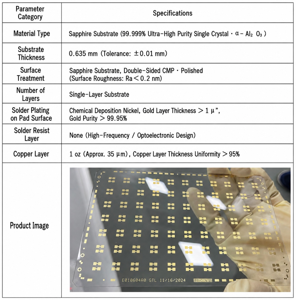
Five Core Scenarios, Precision Empowerment
1. 5G/mmWave RF Circuits: Low Loss, Stable Transmission at High Frequencies
· Industry Pain Points: Devices such as 5G macro base stations, millimeter-wave RF power amplifiers (PAs), and RF front-end modules (FEMs) face technical challenges including high-frequency signal attenuation, excessive insertion loss, difficult impedance matching, and low SMT placement yield.
· Technical Solutions:
· Solder mask-free structure to reduce signal shielding effects and dielectric loss, enhancing high-frequency transmission integrity.
· 1 oz high-uniformity copper foil + high-purity ENIG (Electroless Nickel Immersion Gold) plating to reduce conductor loss and contact resistance, ensuring stable RF signal transmission.
· 99.999% ultra-high purity single-crystal α-Al₂O₃, with stable dielectric constant (εr≈9.4) and dissipation factor tanδ≤0.001, supporting stable operation in millimeter-wave bands above 30 GHz.
· 0.635 mm thickness and ultra-high flatness to meet requirements for high-density interconnect (HDI), fine-line circuitry, and high-precision placement.
· Typical Applications: 5G/6G communication base stations, millimeter-wave terminals, satellite communication RF components—supporting the evolution of high-frequency communication systems.
2. Laser Devices / Optical Communication Modules: High Transmission Efficiency, Integration, and Durability
· Industry Pain Points: Devices such as laser diodes (LDs), optical transceiver modules, and silicon photonics modules face issues like high optical reflection loss, poor optoelectronic integration compatibility, and rapid device aging.
· Technical Solutions:
· Double-sided CMP precision polishing (Ra≤0.2 nm) to reduce Fresnel reflection loss and enhance optical coupling efficiency.
· Optical transmittance >85% in the UV to mid-infrared bands, supporting optoelectronic co-integration on a single substrate for interference-free simultaneous transmission of optical and electrical signals.
· Melting point of 2045°C and Mohs hardness of 9, providing high thermal stability, high mechanical strength, and high wear resistance, significantly extending device service life.
· Typical Applications: High-speed optical communication modules, laser detection systems, automotive LiDAR—supporting the upgrade of the optoelectronics industry.
3. High-End MEMS and Sensors: Precision, Anti-Interference, Adaptability to Complex Conditions
· Industry Pain Points: Industrial-grade and aerospace-grade MEMS devices face bottlenecks such as insufficient detection accuracy, signal crosstalk, excessive latency, and poor adaptability to harsh environments.
· Technical Solutions:
· Single-layer integrated structure that completely eliminates interlayer crosstalk and dielectric hysteresis, with signal transmission delay ≤5 ps.
· Ultra-high flatness and dimensional precision ensuring high-precision bonding and placement of MEMS chips, improving device consistency.
· Excellent chemical stability, acid/alkali resistance, and radiation resistance, meeting the demanding service environment requirements of industrial control, aerospace, and other fields.
·Typical Applications: Pressure sensors, accelerometers, gyroscopes, inertial measurement units (IMUs)—driving high-end sensors toward greater precision and reliability.
4. Medical Endoscopes / Infrared Optical Systems: Sterile, High-Precision, Safe for Diagnosis and Treatment
· Industry Pain Points: Medical endoscopes and infrared optical inspection equipment face challenges including insufficient imaging clarity, electromagnetic interference (EMI), suboptimal biocompatibility, and poor adaptability to sterile environments.
·Technical Solutions:
· Double-sided polished high-transmittance properties support the integrated integration of optical windows and circuitry, enabling high-definition imaging.
· Solder mask-free design reduces electromagnetic interference, while the ENIG plating provides excellent biocompatibility.
· Non-toxic, chemically inert, and resistant to high-temperature sterilization, fully compatible with medical sterile processes and clinical use scenarios.
·Typical Applications: Minimally invasive diagnostic endoscopes, infrared medical testing equipment, clinical diagnostic instruments—supporting the domestic production of high-end medical equipment.
5. High-Power Automotive Electronics Modules: Temperature-Resistant, Vibration-Resistant, Safe and Reliable
· Industry Pain Points: Power modules for new energy vehicles and onboard control units face risks including insufficient high-temperature resistance, weak resistance to vibration and shock, poor stability in high-current transmission, and corrosion in automotive environments.
·Technical Solutions:
· Withstands high temperatures up to 2045°C and Mohs hardness of 9, capable of enduring extreme conditions of high temperature, high vibration, and high dust in engine compartments.
· 1 oz copper layer + ENIG plating supports stable transmission of currents up to ≤5 A, with contact resistance ≤5 mΩ, reducing Joule heating losses.
· High chemical stability and resistance to automotive corrosive media, enhancing long-term system reliability.
·Typical Applications: New energy vehicle power modules, intelligent driving controllers, onboard power systems—ensuring driving safety and low maintenance costs.
Rigorous Process Control to Build a Quality Defense Line
As a precision manufacturing platform focused on high-difficulty, high-reliability, and specialty PCBs, Kinji implements refined process control throughout the entire sapphire substrate production process—from pretreatment, metallization, plating, inspection, to packaging—with scenario-specific quality controls for the five key application areas:
· Metal Adhesion Enhancement: Employing plasma cleaning + ion beam bombardment dual activation, combined with Ti/Cr transition layer deposition, to overcome the challenges of sapphire surface inertness and weak adhesion, achieving metal peel strength of Class 3 (≥0.8 N/mm).
· Precision ENIG Process: Closed-loop control throughout the electroless gold immersion process to eliminate defects such as black pad, skipped plating, and pinholes, with gold layer purity ≥99.95%.
· Ultra-Clean Production Environment: Entire process completed in Class 1000 or higher cleanrooms, with each substrate assigned a unique serial number for full lifecycle traceability.
· Quality System Certification: Certified under ISO 9001 Quality Management System, ensuring product consistency and reliability to international standards.
Customized Services to Precisely Match Differentiated Needs
With standard core parameters as a baseline, Kinji offers comprehensive customized development, with performance optimization tailored to the five major application scenarios:
· 5G/mmWave: Optimize conductor thickness, ENIG layer thickness, and surface impedance to reduce high-frequency insertion loss and return loss; customize dimensions and flatness for seamless production line compatibility.
· Lasers/Optical Communication: Achieve optical transmittance up to >90% and surface roughness optimized to Ra≤0.15 nm; already mass-supplied to leading optical communication companies for 100G optical modules, increasing transmission rates by 12% and reducing failure probability by 30%; custom-developed LD-dedicated substrates for LiDAR to maximize optoelectronic coupling efficiency.
· High-End MEMS/Sensors: Customize dimensions, thickness, flatness, and mechanical strength; enhance EMI resistance and environmental adaptability to meet high-end aerospace and other requirements.
· Medical Endoscopes/Infrared Optics: Enhance biocompatibility, sterile process adaptability, and resistance to high-temperature sterilization; optimize transmittance and circuit layout to meet medical industry access standards.
· Automotive Electronics: Enhance high-temperature resistance, vibration resistance, and power cycling endurance; optimize copper thickness and plating processes to meet automotive-grade high-reliability and high-safety requirements.
Addressing both large-scale production for communications and automotive electronics, as well as small-batch, high-precision customization for lasers, medical devices, and sensors, Kinji provides one-stop sapphire substrate solutions. These help customers reduce R&D costs, shorten iteration cycles, improve product yields, and seize opportunities in the high-end market.
Building on Deep Experience to Support the Self-Reliance of the High-End Electronics Industry
Kinji is a Shenzhen High-Tech Enterprise and an A-level Taxpayer. With over a decade of experience in specialty PCB manufacturing, a well-established industrial chain collaboration system, and multiple core independent intellectual property rights, the company deeply integrates the dielectric, optical, thermal, and mechanical properties of sapphire substrates with the technical requirements of the five major scenarios. This breaks the monopoly of foreign high-end substrate technology and supply chain barriers, providing critical material support for the domestic production of high-end electronic devices in China.
With crystal as the foundation, quality as the soul, and technology as the enabler.
Kinji's sapphire substrates, with their precise parameters, rigorous processes, full-scenario adaptability, and customization services, serve as the core material partner for innovation and upgrading of high-end devices across the five key fields of 5G/mmWave, optical communications, MEMS and sensors, medical optics, and automotive electronics. Together with our customers, we aim to break through critical technical bottlenecks and build a new future of self-reliance for the high-end electronics industry.
trending news
Contact Us