





Sorry, no sales person is available right now to take your call. Pls leave a message and we will reply to you via email as soon as possible.
High-Frequency & High-Speed PCB Material Selection: A Professional Guide from Parameter Understanding to Engineering Implementation
2026-07-30
In conventional perception, PCB substrates are often regarded merely as physical carriers for routing. However, in high-speed digital and microwave/RF design scenarios, this perception can become a critical risk to product performance—PCB materials are, in essence, system-level components that actively participate in signal transmission and thermal-mechanical stress adaptation, with their properties directly determining the electrical performance ceiling and manufacturing yield stability.
As signal rates enter the 56G/112G PAM4 domain and operating frequencies extend into the millimeter-wave band, dielectric loss, timing skew, and impedance mismatch are magnified to an unprecedented extent. Proper material selection ensures controlled performance; a misstep leads to the all-too-familiar industry dilemma: "simulation passes, hardware fails." This challenge is particularly acute in 5G/6G infrastructure, automotive radar, and aerospace RF systems.
I. Core Electrical Parameters: Dk and Df Define Signal Transmission Boundaries
Dielectric Constant (Dk) directly impacts signal propagation velocity and timing alignment accuracy. Selection must evaluate both frequency-domain stability and anisotropy—Dk values in the X-Y plane and Z-axis typically differ, and directly applying generic datasheet parameters in simulation will result in significant discrepancies between modeled and measured performance for microstrip, stripline, and resonant structures. FR-4 maintains stable performance within the 3–10 GHz range, hydrocarbon-ceramic materials excel from 10 to 30 GHz, while PTFE and Panasonic M6/M7 series are tailored for 56G/112G PAM4 and millimeter-wave applications.

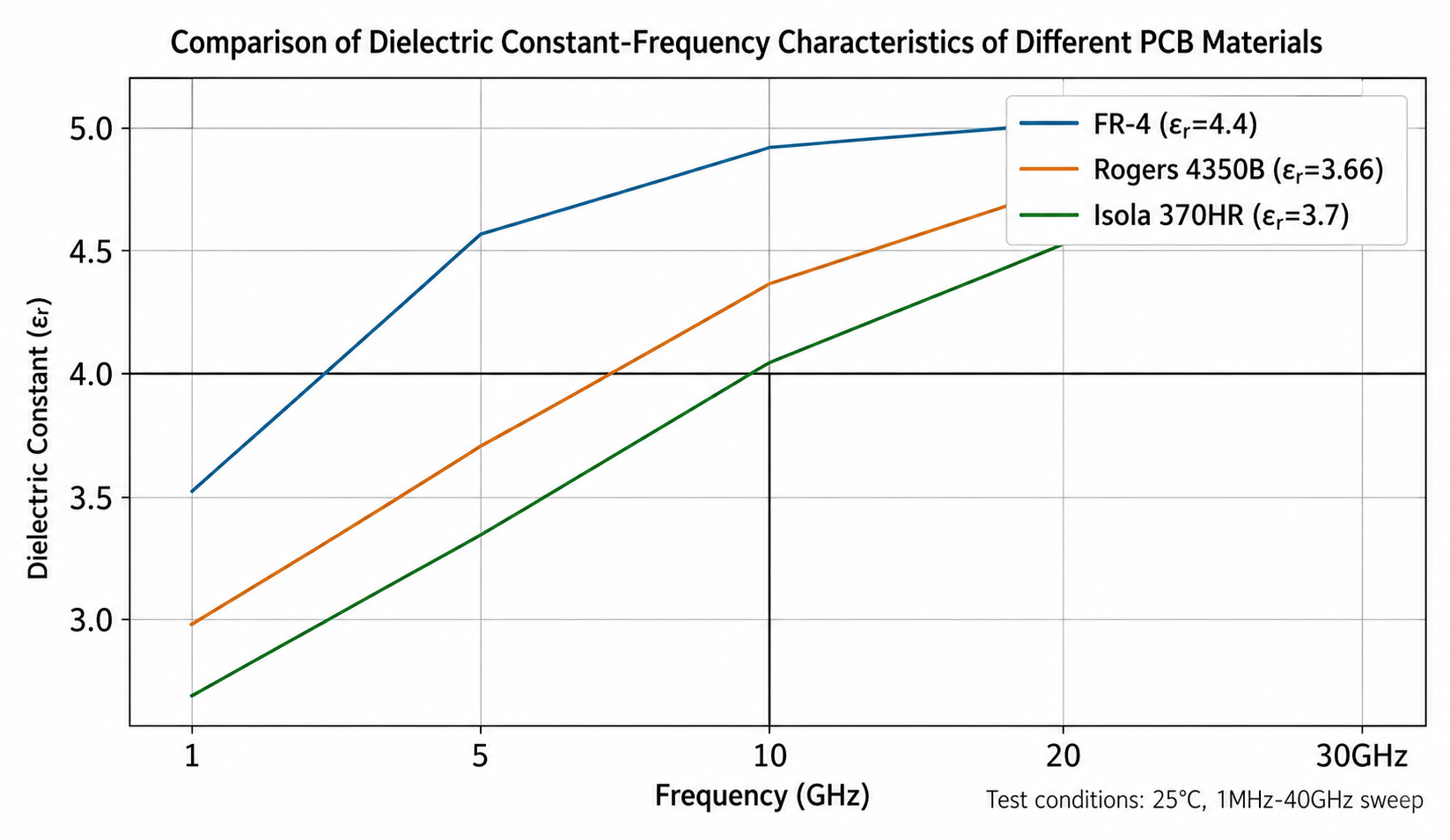
Dissipation Factor (Df) directly constrains channel reach and signal-to-noise ratio, with particularly critical impact on PAM4 high-order modulation links. Engineering selection must consistently reference IPC-TM-650 standardized test data—non-standard single-point values provided by suppliers are prone to causing cross-comparison errors.
II. Conductor Loss: The Hidden Contribution of Copper Foil and Surface Finish
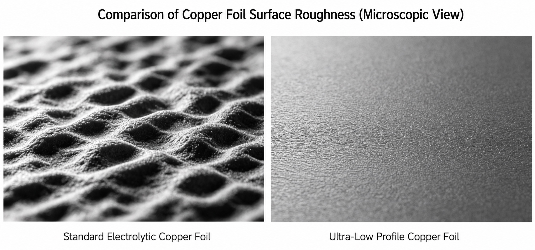
The skin effect concentrates high-frequency current at the conductor surface, making copper foil roughness a non-negligible loss contributor. Per IPC-4562 standards, HVLP (Very Low Profile) and RA (Rolled Annealed) copper foils significantly reduce high-frequency附加 losses, making them the preferred choice for ultra-low-loss links. When operating frequencies exceed 2.4 GHz or trace lengths reach tens of centimeters, the nickel layer in ENIG (Electroless Nickel Immersion Gold) finish introduces additional loss; OSP (Organic Solderability Preservative) and immersion silver finishes, which preserve a flat copper surface, are more suitable for high-speed/high-frequency scenarios.

III. Thermal-Mechanical Reliability and Process Compatibility: Dual Pillars for Performance Realization
Thermal parameters directly determine long-term product reliability: Tg (Glass Transition Temperature) governs structural stability under high-temperature operation, Td (Thermal Decomposition Temperature) reflects resistance to lead-free soldering thermal shock, and CTE (Coefficient of Thermal Expansion) matching prevents via fatigue, barrel cracking, and delamination under thermal cycling—particularly in hybrid FR-4/PTFE stackups, where layer-by-layer CTE matching is mandatory.
High-performance materials can only deliver their promised advantages through precision manufacturing processes. PTFE materials require plasma or sodium etching surface activation, customized drilling parameters, and melt-bond lamination processes; design phase collaboration with PCB manufacturers to validate stackup feasibility and drilling risks is essential to ensure that simulated designs are fully realizable in production.
IV. Mainstream Material Selection Roadmap
| Material Family | Key Characteristics | Typical Applications |
| Enhanced FR-4 | Controlled Dk/Df, cost-effective | ≤10 Gbps / 3–10 GHz |
| Hydrocarbon-Ceramic | Low loss, good processability, hybrid-stackup compatible | 10–56 Gbps / 10–40 GHz |
| PTFE Pure Fluoropolymer | Ultra-low loss, stable Dk across full band | 30–100+ GHz / Millimeter-wave core circuits |
| Panasonic Megtron Series | Ultra-low Df, excellent thermal stability, scalable to standard PCB processes | 25G–112G PAM4 / High-speed backplanes & HPC |
V. Regulatory Compliance and Engineering Implementation
Current material selection must proactively address two major regulatory risks: PFAS (per- and polyfluoroalkyl substances) are subject to the REACH restriction proposal, placing most PTFE materials under compliance uncertainty; certain Megtron formulations contain DBDPE (Decabromodiphenyl ethane), which is listed as an SVHC (Substance of Very High Concern)—target market compliance must be verified in advance.
On the engineering side, practical trade-offs between performance and supply chain reality are essential—premium high-frequency materials typically have extended lead times and limited availability, often addressed through hybrid stackup designs that balance performance and accessibility. Aligning designs with manufacturers' stocked materials during the design phase effectively prevents parameter drift caused by emergency material substitutions. Comprehensive process control must rely on standardized documentation, clearly specifying IPC grades, dielectric thickness and resin content, target Dk/Df values, copper foil grades, test methodologies, and acceptance criteria, while retaining batch numbers and Certificates of Compliance (CoC) to ensure full traceability.

Conclusion
There is no room for compromise in high-frequency and high-speed PCB material selection. Abandoning experience-based heuristics and establishing a structured selection framework—rooted in verifiable data, reproducible testing, and manufacturable processes—is the only path to bridging the industry-wide gap between simulation and measurement. Should you have any questions regarding material selection for your projects, hardware troubleshooting, or compliant material substitution, please contact the Kinji technical team for one-on-one customized solutions.
trending news
Contact Us