





Sorry, no sales person is available right now to take your call. Pls leave a message and we will reply to you via email as soon as possible.
Kinji 6-Layer 6.1mm Stepped-Slot PCB: Unlocking High-Power Reliability Solutions for New Energy Applications
2026-07-28
High-power equipment in sectors such as photovoltaics, energy storage, fast charging, and onboard high-voltage systems have long faced four major challenges: insufficient mechanical strength in thick boards, susceptibility to aging under high temperatures, severe heating during high-current transmission, and structural assembly constraints. The Kinji 6-layer 6.1mm high-precision stepped-slot PCB, combining premium substrate materials, extreme manufacturing processes, and automotive-grade quality control, has emerged as the preferred circuit board solution for high-power new energy applications.
I. Core Specifications at a Glance

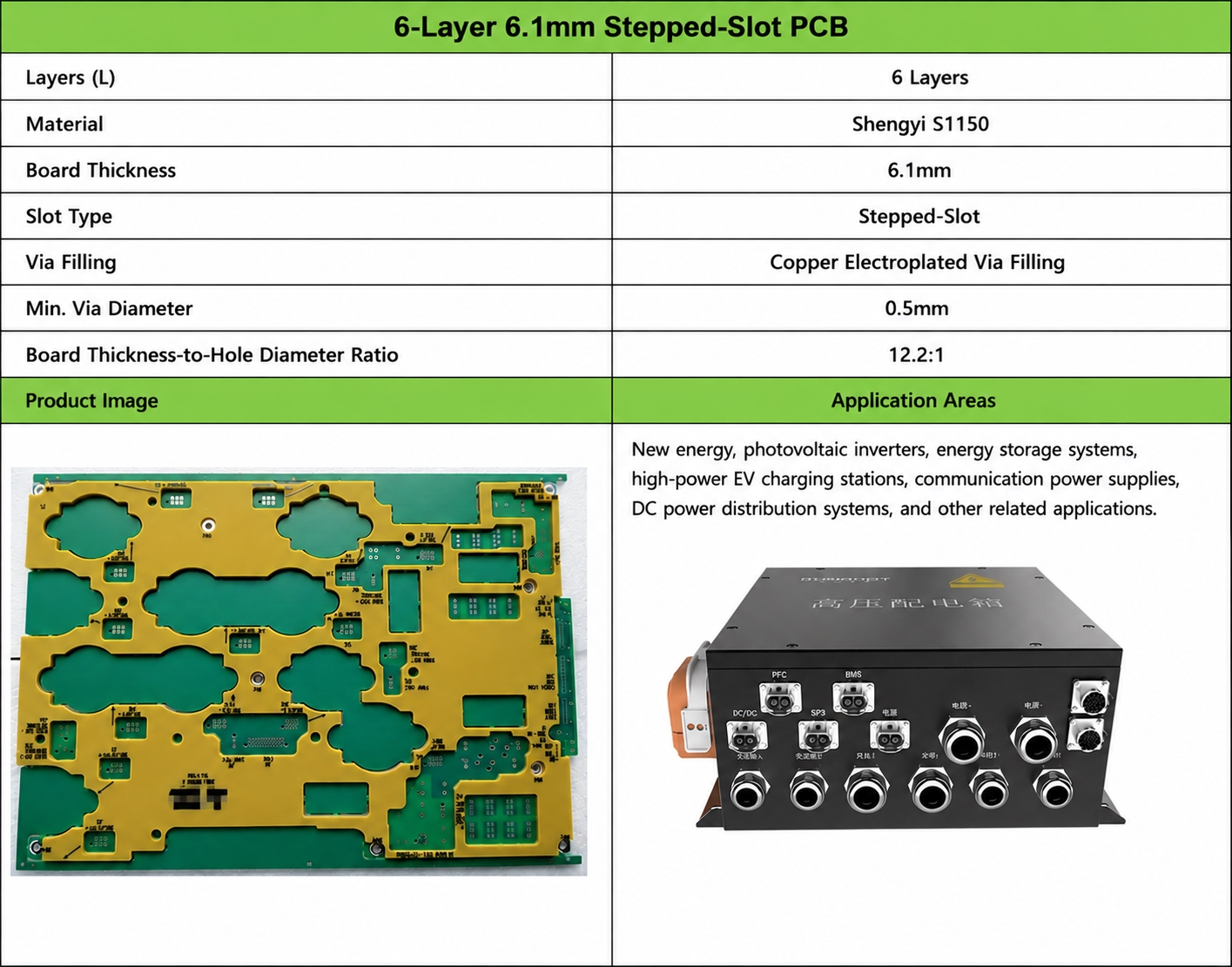 II. Five Core Advantages
6.1mm Ultra-Thick Board + Precision Stepped Slot: Perfect Structural Compatibility
Customized stepped slots precisely accommodate high-power devices, copper busbars, and connectors, ensuring zero interference in internal assembly. The ultra-thick board significantly enhances mechanical strength, resisting deformation and impact—ideal for equipment requiring high stability, such as distribution boxes and inverters.
Shengyi S1150 Premium Substrate: Long-Term Reliability Under Extreme Conditions
With high Tg and excellent heat resistance, the material offers outstanding chemical resistance and insulation properties, stably operating across a wide temperature range of -40°C to 125°C. It resists delamination and aging even under prolonged outdoor high-temperature and continuous operation.
12.2:1 Ultra-High Aspect Ratio + Plated Via Fill: High Current, Low Loss
The 6.1mm thick board enables 0.5mm micro-via drilling, with uniform deep-hole plating for stable conduction. Low interlayer impedance reduces heat generation and transmission losses during high-current operation, supporting thousand-ampere-level high-power scenarios.
Full-Process Smart Manufacturing: Precision and Quality Control
Advanced drilling, plating, lamination, and stepped-slot specialized equipment ensure: drilling accuracy of ±0.02mm and slot verticality ≤0.03mm. The entire process adheres to IATF 16949 automotive-grade standards, with full traceability from incoming materials through each production step to finished product inspection, guaranteeing strong batch-to-batch consistency.
Rapid Delivery and Full Lifecycle Technical Support
72-hour expedited prototyping, flexible capacity for small to large batches; early-stage R&D intervention to optimize stepped-slot layout, thermal management, and thick-board processing. 7×24-hour after-sales support provides one-stop solutions from design to mass production.

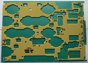
6.1mm 6-Layer High-Precision Stepped-Slot PCB
III. Key Application Scenarios
Photovoltaic Inverters | Energy Storage PCS Systems | Onboard High-Voltage PDU | High-Power DC Fast Chargers | Industrial DC Power Distribution Equipment
IV. Three Benchmark Customer Success Stories
Case 1: Photovoltaic Industry – String Inverter Main Control Board + Power Board Project
1. Requirements Gathering (Full-process follow-up for precise matching)
· Customer Background: A domestic Tier-2 leading PV inverter manufacturer, focusing on residential and C&I photovoltaic applications, primarily producing 110kW–250kW string inverters with annual shipments exceeding 100,000 units. Core markets include domestic industrial parks and emerging overseas markets. This collaboration involved custom development of core PCB components for their next-generation high-efficiency string inverter.
· Initial Requirements Submission: The customer submitted preliminary requirements via the Kinji official website, specifying a 6-layer 6.1mm thick PCB for the inverter's main control and power boards. Core demands were to "resolve PCB warpage and delamination issues in outdoor high-temperature environments, optimize high-current transmission losses, and accommodate the compact layout of IGBT modules and heat sinks."
· In-Depth Requirements Analysis: Within 3 working days, the Kinji technical team engaged with the customer via online meetings and preliminary sample testing, refining requirements as follows: ① substrate must withstand prolonged outdoor operation at up to 65°C and start reliably at -40°C, complying with IEC 61215 standards; ② the 6.1mm thick board must provide excellent mechanical strength to prevent warpage in long-term outdoor use; ③ stepped-slot design to precisely clear IGBT module pins and heat sinks, minimizing assembly gaps; ④ support 300A+ high-current transmission with interlayer loss below industry average; ⑤ prototype lead time ≤72 hours, batch delivery ≤7 days per batch, with annual volume of approximately 30,000 units.
· Requirements Confirmation and Solution Proposal: Based on the customer's needs, Kinji proposed a customized solution using Shengyi S1150 high-heat-resistance substrate, 12.2:1 aspect ratio + plated via fill process, and stepped-slot geometry tailored to the customer's inverter layout drawings. Preliminary process parameters and delivery plans were submitted, with customer confirmation and prototype kickoff within 3 working days.
2. Process Challenges (Pinpointing Pain Points and Core Difficulties)
Given the outdoor operating conditions and product characteristics, four core process challenges were identified, all common pain points in thick-board stepped-slot PCB manufacturing:
· Thick-Board Deformation: The 6.1mm ultra-thick board (6-layer lamination) is prone to uneven layer stress during pressing, causing finished board warpage. If warpage exceeds 0.3mm, it cannot fit the inverter's compact internal layout, affecting IGBT assembly and heat dissipation.
· High-Temperature Reliability: Wide temperature fluctuations outdoors (-40°C to 65°C) can cause ordinary substrates to age and delaminate, especially under prolonged high-temperature operation, potentially increasing conduction impedance and compromising high-current transmission stability, leading to inverter failures.
· Stepped-Slot Precision: The stepped slots must precisely clear IGBT modules and heat sinks, requiring groove depth tolerance ≤0.03mm, verticality ≤0.02mm, and burr-free, chip-free slot edges; otherwise, assembly gaps will be too large, reducing heat dissipation efficiency and structural stability.
· High-Current Transmission Loss: The power board must carry 300A+ currents. Uniform plating in 0.5mm deep vias in the 6.1mm board is difficult to achieve; uneven plating increases interlayer impedance and transmission losses, lowering inverter conversion efficiency.
3. Solution Implementation (Technical Breakthroughs and Full-Process Control)
A dedicated task force was established, integrating R&D, production, and quality departments to develop targeted solutions and ensure issue resolution:
· Anti-Deformation Solution: Optimized lamination parameters using "stepwise pressing + constant-temperature curing," with pressing temperature at 170°C±5°C and pressure gradients of 0.3MPa→0.5MPa→0.8MPa, each held for 30 minutes to avoid uneven stress. Pre-baking of substrates (120°C, 2 hours) removed moisture, reducing deformation risk. Finished boards were clamped during cooling to control warpage within 0.2mm.
· High-Temperature Reliability Solution: Strict selection of Shengyi S1150 high-Tg (150°C) substrate with excellent thermal stability and aging resistance. 100% incoming material inspection ensured compliance with IEC 61215. Optimized layer spacing and copper thickness enhanced heat dissipation and high-temperature tolerance.
· Stepped-Slot Precision Solution: Utilized state-of-the-art high-precision stepped-slot machining centers with CCD vision positioning (accuracy ±0.01mm). 3D customer layout drawings were imported for simulation to optimize slot dimensions and toolpaths. Real-time sampling (1 per 10 boards) inspected slot depth, verticality, and edge quality; burrs were removed via precision polishing.
· High-Current Loss Reduction Solution: Improved plated via fill using "acidic copper plating + pulse plating," with current density controlled at 2.5A/dm² and extended plating time of 60 minutes to ensure uniform coating (≥25μm). Hole wall roughness was optimized to reduce contact impedance and transmission losses. Prototype testing fine-tuned parameters to meet customer requirements.
· Delivery Assurance: Expedited prototyping with dedicated production lines, delivering samples within 72 hours along with inspection reports. Mass production utilized fully automated parallel lines with IATF 16949 quality control and real-time sampling at each step to ensure consistency. Logistics were coordinated to guarantee on-time batch deliveries.
4. Validation Data (Quantified Metrics Demonstrating Value)
The customer conducted comprehensive testing on prototypes and mass-produced units per IEC 61215 and agreed specifications. All metrics met requirements, and the project passed validation:
| Mechanical Performance | Result | Requirement |
| Warpage | 0.15mm | ≤0.3mm |
| Impact strength | ≥15J/cm² | No fracture/deformation |
| Stepped-slot accuracy | Depth error 0.02mm, verticality 0.015mm; burr-free | Assembly gap ≤±0.04mm (target ±0.05mm) |
| High-Temperature Reliability | Result |
| Thermal cycling (-40°C~65°C, 100 cycles) | No delamination/cracking; stable impedance |
| Long-term high temp (65°C, 8000 hrs) | No substrate aging, pad detachment, stable conduction |
| Damp heat (40°C, 95% RH, 1000 hrs) | No oxidation, short circuits; good insulation |
| High-Current Transmission | Result | Industry Avg |
| 300A continuous (24 hrs) | Temp rise 11°C | 20°C |
| Transmission loss reduction | 18% lower than customer's previous PCB | — |
| Inverter conversion efficiency | Improved from 98.2% to 98.5% (+0.3%) | — |
| Delivery Performance | Result |
| Prototype lead time | 72 hours (met) |
| Batch delivery | 6 days/batch (met) |
| Batch yield | 99.8% (target ≥99.5%) |
| Traceability | Unique code per board tracking material, process, and test data |
Conclusion: All indicators met customer requirements and industry standards. The project passed validation, mass production is ongoing, customer feedback is positive, and expansion of cooperation is planned.
Case 2: Energy Storage – Southeast Asian Energy Storage PCS Power Unit
· Customer: Major Southeast Asian energy storage system integrator
· Requirements: Withstand high temperature and humidity, endure bidirectional 500A frequent charge/discharge shocks
· Results: No conduction degradation after thousands of cycles; stepped-slot design improved heat dissipation by 22% when paired with thermal modules; full CE/CQC certification; stable monthly capacity exceeding 5,000 units, supporting a 1GWh energy storage project.
Case 3: High-Power DC Fast Charging – 180–360kW Charging Piles
· Customer: Leading domestic charging pile OEM
· Requirements: Low temperature rise at kiloampere-level currents, strong interference immunity, complex internal structure accommodation
· Results: Temperature rise of only 15°C at 1000A continuous operation (vs. industry standard of 25°C); passed national EMC immunity tests; rapid structural iterations shortened the overall project timeline by 15 days.
The above three projects validate the core competitiveness of Kinji's 6.1mm 6-layer high-precision stepped-slot PCB, while demonstrating the company's technical prowess, production capabilities, and full-process service advantages:
1. Technical Strength: Expertly addresses thick-board deformation, high-current transmission, high-precision stepped-slot machining, and high-temperature/humidity adaptation through customized process solutions for diverse scenarios.
2. Production Capability: Fully automated lines support rapid prototyping (as fast as 48 hours) and volume delivery, with automotive-grade quality control and stable batch yields above 99.7%, accommodating varying customer capacity needs.
3. Service Advantage: Full-process technical team engagement, rapid response to customer requirements, efficient iteration support, and assistance with overseas certifications and standards compliance—delivering an integrated "product + service" package that reduces R&D and production costs while accelerating project deployment.
Choose Kinji – More Than Just a Custom High-Precision Stepped-Slot Thick PCB:
✔ Premium substrate + extreme processes – suitable for all new energy high-power harsh conditions
✔ Automotive-grade quality control with full domestic and international certifications – worry-free export and automotive projects
✔ Rapid prototyping + flexible mass production – fits R&D iterations and large-scale delivery
✔ Full-process technical support – from design optimization to mass production, we guide you every step of the way
trending news
Contact Us