





Sorry, no sales person is available right now to take your call. Pls leave a message and we will reply to you via email as soon as possible.
Analysis of HDI High-Order Board Levels: A Complete Guide to First-Order, Second-Order, Third-Order, and AnyLayer Blind Buried Via Processes
2026-07-28
Many engineers have misconceptions about the "level" concept of HDI (high-density interconnect) boards. In fact, the criterion is extremely simple: the level is determined by the number of fiberglass dielectric layers that a laser blind via penetrates in a single shot—one layer is first-order, two layers is second-order, and three layers is third-order. AnyLayer, on the other hand, breaks free from the level framework. It uses a layer-by-layer build-up approach to achieve free interconnection between any two layers and is the core process for high-end precision PCBs.
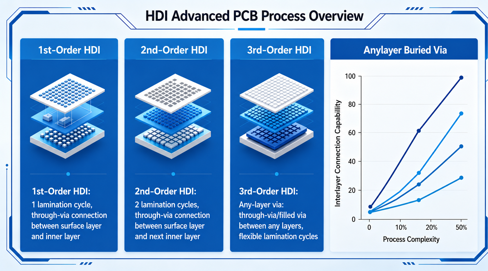
I. First-Order HDI: Entry-Level Basic Process
Process Principle
First, complete the overall board base lamination. Then use a laser from the surface layer to burn through the first layer of copper foil and the insulating dielectric, so that the blind via stops precisely on the surface of the first inner-layer copper foil (without penetrating the copper layer). This is followed by a single electroplating filling step to complete the conduction. The entire process requires only "single drilling + single hole filling," with a simple workflow. Alignment tolerances are generous; slight deviations do not affect quality, and yield is very easy to control.
Application Scenarios
It is mostly used in areas that do not demand high wiring density or strict board thickness precision, such as older entry-level mobile phones, ordinary industrial control boards, and conventional digital device mainboards.

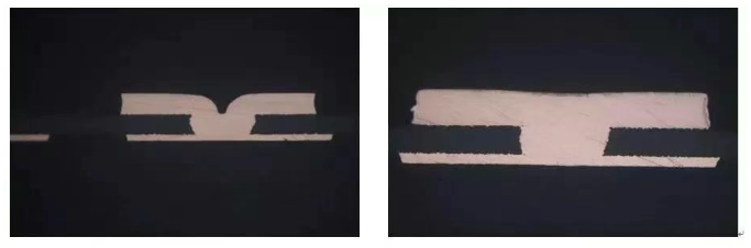
II. Second-Order HDI: Dual Laser Drilling Process (Mid-to-High-End Mainstream)
Second-order HDI requires conducting through two dielectric layers. Single-shot laser energy often cannot balance hole quality and aspect ratio, so the industry generally adopts either the staggered stacked via method or the direct stacked via method.
Staggered Stacked Via Method (taking L1-L3 conduction as an example)
First, drill L2-L3 blind vias and fill them with electroplated copper. After lamination, drill L1-L2 blind vias, with the upper and lower via positions offset from each other and not overlapping.
Advantages: high yield and strong fault tolerance.
Disadvantages: requires reserved offset space, occupying routing area.
Direct Stacked Via Method (taking L1-L3 conduction as an example)
The initial process is the same, but the second drilling must precisely align with the lower via position so that the upper and lower vias are vertically continuous, forming a straight blind via that penetrates two dielectric layers.
Core challenge: the flatness of the first copper filling must be extremely high—if the bottom filled hole has depressions or protrusions, the second laser will receive uneven heat, easily leading to incomplete drilling, penetration of the bottom copper foil, or damage to the via wall.
The key quality control focus is on hole-filling electroplating and board surface grinding. Most factories have low second-order yields precisely because the flatness at the stacked via locations does not meet standards.

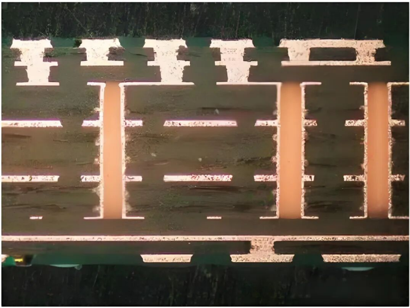
III. Third-Order HDI: The High-End Ceiling of Traditional Level-Based Processes
Third-order HDI can penetrate three dielectric layers with a single laser shot (e.g., L1-L4) or achieve multilayer interconnection through three stacked vias, significantly increasing process difficulty.
Two Major Core Difficulties
Laser parameters are extremely hard to control: insufficient energy means the dielectric is not fully burned through; excessive energy penetrates the copper foil at the via bottom or causes the via wall to deform into a flared shape, affecting conduction reliability.
Multilayer alignment precision is demanding: three drilling operations must align layer by layer with the embedded landing pads in the inner layers, while board thermal expansion/contraction and dimensional variations can easily cause via position shift.
Using staggered stacked vias can reduce some difficulty, but as the number of layers increases, the space required for offset keeps growing, severely compressing the routing area and highlighting design limitations.
IV. AnyLayer: Ultimate Precision Process with Layer-by-Layer Build-Up
AnyLayer is not a simple extension of third-order; it represents a fundamental change in manufacturing logic. Traditional HDI first makes the core board and then adds outer layers, whereas AnyLayer uses a layer-by-layer build-up mode: with each layer of copper foil laminated, laser drilling, vacuum copper filling electroplating, and ceramic plate grinding are performed, cycled more than ten or even more than twenty times, ultimately achieving unrestricted interconnection between any two layers. This process is the unquestionable choice for flagship smartphone mainboards (such as Apple and Huawei).
Three Major Process Challenges
Ultra-high precision alignment compensation: drilling on each layer must match the original design data in real time, requiring a CCD dynamic expansion/contraction compensation system to eliminate cumulative multilayer offset.

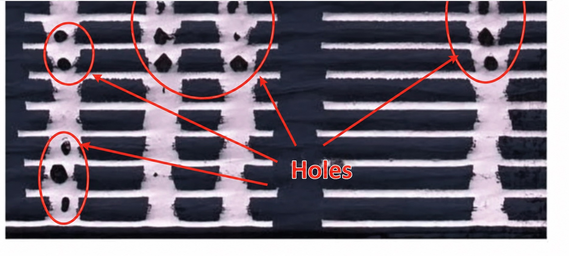
Defect-free copper filling and ultra-flat grinding: all blind vias must be 100% filled with solid copper, with no voids, and then ground with ceramic plates to ultra-low roughness; otherwise, subsequent lamination will result in delamination, blistering, or peeling.
Extremely uniform overall board thickness: after more than ten cycles of electroplating, grinding, and lamination, the overall board thickness variation must be controlled within ±5%, with precision comparable to semiconductor packaging levels.
Cost and Advantages
AnyLayer enables ultra-thin mainboards and ultra-high wiring density, with significantly improved performance and integration. However, its production cost is 3 to 5 times that of first-order HDI, with lengthy process steps and longer lead times, making it suitable only for high-end precision equipment.
V. Quick Comparison Summary of the Four Processes:
The essence of the level is a measure of the number of dielectric layers penetrated by a blind via. Difficulty increases from first-order to third-order, while AnyLayer overturns the traditional "core board stacking" logic with "layer-by-layer accumulation," achieving a qualitative leap in design freedom. When selecting a process, it is necessary to weigh performance requirements, process yield, and cost budget in order to precisely match the product positioning.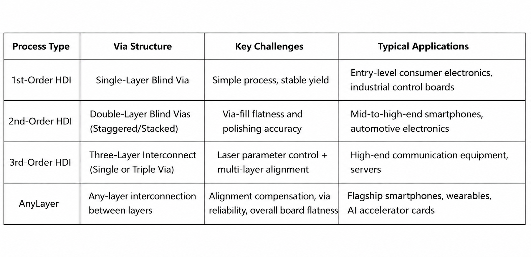 For further information about high-order HDI process capabilities or customized solution recommendations, please feel free to contact us. Our technical support team is ready to assist you.
trending news
Contact Us