





Sorry, no sales person is available right now to take your call. Pls leave a message and we will reply to you via email as soon as possible.
How Kinji Helped an EV Power Electronics Client Cut Board Temperatures by 22°C with Heavy Copper Ceramic PCBs
2026-07-24
Introduction
The automotive industry’s rapid migration to 800V EV architectures, combined with the adoption of wide‑bandgap silicon carbide (SiC) power semiconductors, has fundamentally reshaped thermal management requirements. SiC MOSFETs deliver superior switching speed and efficiency, but they concentrate heat into much smaller die areas, creating intense localised hotspots that legacy printed circuit boards (PCBs) struggle to handle.
Many OEMs and Tier 1 suppliers find themselves caught between rising power density targets and the physical limits of conventional metal‑core PCBs (MCPCBs). Persistent overheating leads to forced power derating, accelerated component ageing, and reduced system reliability – especially under sustained high‑torque or high‑ambient driving conditions.
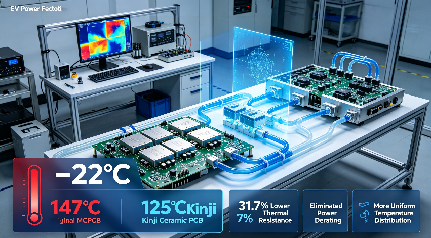
A European EV power electronics developer faced exactly this challenge on its next‑generation traction inverter prototype. Initial MCPCB‑based designs showed peak substrate temperatures of 147°C during continuous full‑load bench testing – well beyond the safe long‑term operating threshold. After incremental tweaks to thermal interface materials and cooling layouts produced only marginal gains, the client turned to Kinji’s automotive power substrate engineering team for a fundamental redesign. The solution: a custom heavy copper ceramic PCB leveraging Kinji’s DBC (Direct Bonded Copper) technology on an aluminium nitride (AlN) base.
The outcome was definitive – independent bench verification recorded a 22°C reduction in peak board temperature under identical test conditions, eliminating power derating and significantly extending projected module life. This article details the technical journey, the substrate innovations applied, and the measurable business value delivered.
Client Background & Core Challenges
The customer is a Tier 1 supplier developing high‑density traction inverters for passenger EVs targeting 800V battery systems. Their design employs parallel SiC MOSFETs to maximise power density while reducing overall system weight.
Before engaging Kinji, the project was constrained by four critical issues:
Severe hotspot formation – The original MCPCB’s polymer dielectric layer limited vertical heat conduction, causing heat to accumulate directly beneath the SiC dies. Peak board temperature reached 147°C under standard test cycles.
Forced power derating – To keep junction temperatures within safe limits, the control software capped continuous output power by 12%, directly compromising vehicle acceleration and charging performance.
Thermal cycling reliability risks – The wide operational range (–40°C to 125°C) induced thermal stress mismatches between the FR‑4/metal substrate and the SiC chips, elevating the risk of solder fatigue and eventual delamination.
Fixed mechanical envelope – The inverter housing and liquid‑cooling loop were already finalised; any thermal improvement had to come from substrate‑level innovation, not from larger heatsinks or increased coolant flow.
Previous optimisation attempts – upgrading thermal interface materials, fine‑tuning coolant flow rates, and adjusting component placement – delivered only 3–6°C reductions, insufficient to meet specifications. The team recognised that only a fundamental substrate material and construction change could bridge the gap, prompting a formal collaboration with Kinji.
Kinji’s Technical Approach: Heavy Copper Ceramic PCB Solution
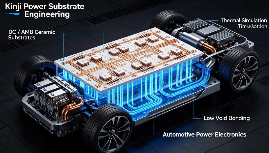
Kinji’s engineering team initiated the cooperation with a joint thermal mapping exercise and finite element analysis (FEA) review, precisely identifying the heat‑flow bottlenecks in the existing layout. The proposed solution combined a high‑performance ceramic dielectric with zone‑based heavy copper metallisation, built upon Kinji’s mature DBC manufacturing workflows, fully aligned with AEC‑Q automotive reliability standards.
1. Substrate Material Selection
After benchmarking alumina (Al₂O₃), aluminium nitride (AlN), and silicon nitride (Si₃N₄), Kinji recommended a 0.63 mm AlN DBC ceramic substrate for this inverter application, based on the following attributes:
Thermal conductivity of 170 W/m·K – over 500× higher than standard FR‑4, creating an efficient vertical heat path.
Coefficient of thermal expansion (CTE) matched to SiC – minimises thermomechanical stress during power cycling.
High dielectric strength – satisfies 800V automotive isolation requirements with adequate safety margins.
2. Zone‑Based Heavy Copper Circuit Optimisation
Rather than applying uniform copper thickness, Kinji implemented a differentiated copper strategy:
Power device areas – 6 oz (210 μm) bonded copper, serving simultaneously as a high‑current conductor and a planar heat spreader.
Signal routing zones – thinner copper to control parasitic capacitance and reduce unnecessary thermal mass.
Precision edge profiling and copper fillet control – minimises localised stress risers and prevents copper delamination over thousands of thermal cycles.
3. DFM & Thermal Path Refinement
Several design‑for‑manufacturing (DFM) adjustments compounded the thermal benefits:
Optimised copper pattern geometry to equalise current sharing across parallel SiC devices, eliminating current‑hogging hotspots.
Controlled ceramic‑copper bonding interface with strict low‑void standards – preserving direct vertical heat conduction.
Professional guidance on land pattern adjustments to maximise the contact area between SiC packages and heavy copper pads.
Kinji delivered validated engineering samples within the agreed timeline, accompanied by comprehensive laser flash analysis (LFA) thermal characterisation reports, enabling the client to proceed directly to bench validation.
A Broader Perspective: Ceramic Substrate Technologies in Power Electronics
While DBC (Direct Bonded Copper) was the optimal choice for this traction inverter application due to its excellent thermal performance and cost‑effectiveness, it is worth noting the broader landscape of ceramic substrate technologies that serve the power electronics industry.
DPC (Direct Plating Copper) is another key ceramic metallisation工艺. Unlike DBC’s high‑temperature bonding process, DPC employs semiconductor‑grade microfabrication techniques: it begins with vacuum sputtering (e.g., magnetron sputtering) to deposit a Ti/Cu seed layer on the ceramic surface, followed by electroplating to build up the copper thickness. The entire process is conducted below 300°C, making it a low‑temperature process that avoids thermal stress on the ceramic substrate. DPC excels in high circuit precision – line width and spacing can be achieved as fine as 30–50 μm – and supports vertical interconnections through vias. It is widely used in applications demanding fine‑line routing and compact footprints, such as high‑power LEDs, semiconductor lasers, 5G communication modules, and certain automotive electronic packages. However, for high‑power traction inverters requiring thick copper layers (typically 100–300 μm or more) for current carrying and heat spreading, DBC and AMB remain the preferred choices due to their superior copper thickness capability and metallurgical bonding strength.
For applications requiring three‑dimensional multilayer integration, HTCC (High Temperature Co‑fired Ceramic) and LTCC (Low Temperature Co‑fired Ceramic) offer distinct capabilities. HTCC involves co‑sintering multiple layers of ceramic tape with high‑melting‑point metals such as tungsten, molybdenum, or molybdenum‑manganese at temperatures between 1500°C and 1850°C. This yields substrates with exceptionally high mechanical strength, chemical stability, and hermeticity, making HTCC suitable for demanding封装 applications like ceramic packages for MEMS, optical communications, and high‑reliability microwave devices. LTCC, by contrast, uses ceramic tapes blended with low‑melting‑point glass frit, enabling co‑firing with high‑conductivity metals such as silver, gold, and copper at temperatures below 950°C. LTCC supports multi‑layer structures with embedded passive components (capacitors, inductors, resistors) and is extensively used in RF front‑ends, satellite radar, and autonomous driving sensors where high‑frequency performance and integration density are paramount.
For power electronics applications like EV traction inverters, where the primary requirements are high thermal conductivity, thick copper for current handling, and thermomechanical reliability under power cycling, DBC and AMB remain the dominant choices. Kinji’s core expertise lies in these application‑optimised substrate technologies, with DBC serving as the proven workhorse for this 22°C temperature‑reduction case.
Bench Test Results: Verified 22°C Temperature Drop
All validation tests were performed on the same test bench, with identical liquid cooling parameters, same SiC power modules, and a consistent continuous full‑load duty cycle.
| Parameter | Original MCPCB Solution | Kinji Heavy Copper Ceramic PCB | Improvement |
|---|---|---|---|
| Peak board surface temperature | 147°C | 125°C | −22°C |
| Thermal resistance (device to cold plate) | 0.41 °C/W | 0.28 °C/W | 31.7% lower |
| Maximum sustainable continuous power | Derated 12% | Full rated power | Derating eliminated |
| Hotspot temperature gradient across substrate | 21°C | 9°C | More uniform distribution |
Beyond the headline 22°C reduction, the Kinji substrate delivered two additional strategic advantages:
Extended operational lifetime – Lower sustained temperatures slow electromigration, solder joint creep, and package ageing, significantly improving projected mean time between failures (MTBF).
Thermal headroom for harsh environments – The extra margin ensures stable operation in high‑ambient climates and during repeated hill‑climbing drive cycles, without triggering thermal protection.
Why Kinji Heavy Copper Ceramic PCBs Outperform Traditional Power Substrates
Most EV designers default to MCPCBs for power circuits, but these are fundamentally limited by their polymer dielectric layers, which have poor thermal conductivity. Kinji’s heavy copper ceramic structures overcome this limitation through:
High‑thermal‑conductivity ceramic – creates a direct vertical heat highway from device to cold plate.
Thick bonded copper – spreads heat laterally to erase sharp hotspots and reduce peak temperatures.
Metallurgical bonding – between copper and ceramic ensures stable thermal performance over the entire automotive service life.
High voltage isolation – supports 400V and 800V EV platforms with robust dielectric strength.
High current capability – supports continuous high currents without excessive I²R heating.
Kinji offers multiple manufacturing routes, tailored to application requirements:
DBC (Direct Bonded Copper) – cost‑effective for mid‑to‑high power inverters, on‑board chargers (OBC), and DC‑DC converters with standard thermal cycling demands.
AMB (Active Metal Brazing) – premium solution for Si₃N₄ substrates targeting extreme thermal cycling and the highest reliability requirements (e.g., automotive main traction inverters with ultra‑long warranty periods).
DPC (Direct Plating Copper) – available for applications requiring fine‑line precision and high routing density, complementing the thick‑copper DBC/AMB portfolio.
Business Outcomes for the EV Client
The successful implementation of Kinji’s heavy copper ceramic PCB delivered tangible business results:
Spec compliance achieved – The inverter prototype passed all thermal validation tests without requiring any mechanical redesign of the cooling system or enclosure.
Development cycle saved – Avoiding costly, time‑consuming hardware iterations on cooling assemblies reduced overall project risk and accelerated time‑to‑market.
Product competitiveness enhanced – Full‑power continuous operation translates directly to better real‑world vehicle performance, a key differentiator in the crowded EV market.
Scalable platform – The validated ceramic heavy copper design is now being reused across the client’s future 800V OBC and auxiliary converter programmes, amortising engineering investment.
Conclusion
As EV power electronics continue their trajectory toward higher voltages, higher power densities, and widespread SiC adoption, thermal management can no longer be an afterthought. Incremental cooling tweaks have diminishing returns; the substrate architecture itself becomes the critical lever for controlling hotspot temperatures.
In this real‑world traction inverter project, Kinji’s custom heavy copper ceramic PCB cut peak board temperature by 22°C, eliminated mandatory power derating, and created critical thermal safety margin – all within the existing mechanical envelope. For OEMs and Tier 1 suppliers racing to commercialise next‑generation EV power converters, Kinji’s application‑focused engineering offers a proven, scalable path to balance power density, thermal stability, and long‑term automotive reliability.
Are you struggling with persistent hotspots, over‑temperature alerts, or power derating on your EV inverter, OBC, or DC‑DC designs?
Contact Kinji’s power substrate engineering team to explore custom heavy copper DBC / AMB ceramic PCB thermal optimisation tailored to your project.
Frequently Asked Questions
Q1: What is a heavy copper ceramic PCB from Kinji?
A: Kinji heavy copper ceramic PCBs encompass DBC (Direct Bonded Copper) and AMB (Active Metal Brazing) substrates. They combine high‑thermal‑conductivity ceramic bases (Al₂O₃, AlN, or Si₃N₄) with thick bonded copper circuits. Unlike conventional MCPCBs, there is no low‑conductivity polymer dielectric layer, enabling far superior vertical heat dissipation for high‑power SiC and IGBT applications.
Q2: Can heavy copper ceramic PCBs really reduce board temperature by more than 20°C, as in this EV case?
A: The actual temperature improvement depends on power density, cooling structure, substrate material, and layout. In this verified traction inverter project, Kinji’s custom AlN DBC solution achieved a confirmed 22°C peak temperature reduction under identical test conditions. For different power levels and packaging forms, Kinji engineers perform pre‑simulation to predict achievable thermal gains before sample production.
Q3: What’s the difference between Kinji DBC and AMB ceramic substrates?
A: Kinji DBC uses direct copper bonding technology – ideal for mid‑to‑high power EV inverters, OBC, and DC‑DC converters with standard thermal cycling demands, offering excellent cost‑performance. Kinji AMB employs active metal brazing, providing stronger bonding strength and superior resistance to thermal shocks, making it suitable for Si₃N₄ substrates in premium automotive and industrial power modules with stringent long‑term reliability requirements.
Q4: What about DPC – does Kinji offer that as well?
A: Yes. In addition to DBC and AMB, Kinji also supports DPC (Direct Plating Copper) substrates for applications that demand fine‑line precision and high routing density. DPC utilises semiconductor‑grade sputtering and electroplating processes to achieve line widths down to 30–50 μm, making it suitable for compact power modules, optical devices, and high‑density interconnects where space is at a premium.
Q5: Are ceramic PCBs suitable for 800V SiC EV power electronics?
A: Yes. Kinji’s Al₂O₃, AlN, and Si₃N₄ ceramic substrates support high isolation voltages and closely match the CTE of SiC chips. They effectively relieve thermal stress during frequent power cycling, making them an ideal substrate choice for next‑generation 800V traction inverters and on‑board chargers.
Q6: If my product housing and cooling structure are already fixed, can Kinji still improve thermal performance?
A: Exactly the scenario of this EV client. When mechanical space cannot be modified, optimising the power substrate is one of the most efficient solutions. Kinji can perform layout optimisation, select appropriate ceramic materials, and configure heavy copper metallisation schemes to maximise heat spreading without changing existing enclosures or cooling loops.
Q7: Does Kinji provide thermal simulation support before making samples?
A: Yes. Kinji offers pre‑project thermal simulation and DFM review services. Our team analyses hotspot distribution, thermal resistance, and current‑sharing risks, proposing targeted substrate material and copper design recommendations to avoid trial‑and‑error and shorten customer development cycles.
Q8: What copper thickness options does Kinji support for ceramic substrates?
A: Kinji supports flexible heavy copper solutions ranging from 3 oz up to 10 oz on DBC and AMB substrates. We employ zone‑based design strategies – thicker copper for power switching regions and thinner copper for signal circuits – balancing high‑current transmission, heat spreading, and parasitic parameter control.
Q9: Are Kinji ceramic substrates qualified for automotive applications?
A: Kinji manufactures ceramic power substrates following automotive‑grade process standards. We can collaborate with customers to complete thermal cycling, power cycling, insulation resistance, and void‑rate testing to meet reliability verification requirements for EV Tier 1 and OEM projects.
Q10: How do I start a sample project with Kinji for thermal optimisation evaluation?
A: Simply send us your circuit layout, power parameters, cooling conditions, and target thermal indicators. Kinji’s power substrate engineers will conduct a technical review, provide material and structural recommendations, and arrange prototype samples for your bench testing. Contact us today to begin.
trending news
Contact Us