





Sorry, no sales person is available right now to take your call. Pls leave a message and we will reply to you via email as soon as possible.
Five Core Technical Challenges and Solutions for High-Frequency PCB Prototyping (With Real-World Case Studies)
2026-07-23
Introduction: Where Exactly Are the Core Pain Points in High-Frequency PCB Prototyping?
The performance ceiling of high-end equipment such as 5G communications, millimeter-wave radar, satellite navigation, and high-speed optical modules depends critically on the process precision and material stability of high-frequency PCBs. Compared with conventional FR-4 circuit boards, high-frequency PCBs impose requirements on substrate physical properties, manufacturing tolerances, and process compatibility that are orders of magnitude higher, and they are by no means a simple extension of ordinary PCB production lines.
In the industry, circuit boards with operating frequencies ≥300 MHz are generally classified as high-frequency PCBs. When signal frequencies enter the GHz range, the traces on the board are no longer ordinary conductive paths but high-precision signal transmission lines. At this point, three key physical parameters directly determine design success or failure:
Dielectric constant (Dk) and dissipation factor (Df) — governing signal propagation speed and dielectric attenuation;
Coefficient of thermal expansion (CTE) and copper foil surface roughness (RMS) — dominating impedance consistency and long-term reliability.
During prototyping, improper substrate selection, loss of impedance control, and mismatched surface finishes often directly trigger chain problems such as excessive signal attenuation, shortened communication range, soldering failures, and even severe performance drift with temperature.
As a "specialized, refined, distinctive, and innovative" enterprise deeply engaged in high-precision, high-difficulty, and special-process PCB manufacturing, Kinji has 29 years of volume-production experience and a 200-person professional technical team. Relying on two intelligent production bases in Shenzhen and Jiangxi, its monthly production capacity reaches 100,000 m². Based on front-line engineering practice, this article thoroughly analyzes five typical technical difficulties in high-frequency PCB prototyping and provides implementable design and manufacturing solutions.

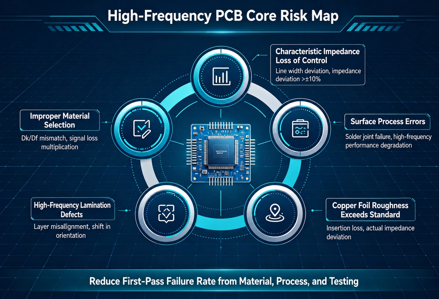
Challenge 1: Improper Board Material Selection — Mismatched Substrate Adaptability, Resulting in Significant Overall Performance Degradation
1. Problem Manifestation
After high-frequency PCB prototyping, it is common to see signal insertion loss severely exceeding limits, significant high-frequency attenuation, and communication distance far below the design value. Even after switching to multiple board manufacturers for repeated trial production, the problem persists.
2. Root Cause Analysis
Conventional FR-4 materials have Dk of 4.2–4.8 and Df of 0.015–0.025. Under high-frequency operating conditions, dielectric polarization losses rise sharply, easily converting high-frequency signal energy into heat and causing waveform distortion and substantial energy dissipation. Dedicated high-frequency materials must simultaneously possess low dielectric constant, low dissipation factor, and excellent stability over wide temperature and frequency ranges — all three are indispensable.
3. Solution
Strictly match dedicated high-frequency materials according to the operating frequency gradient, balancing performance and cost:
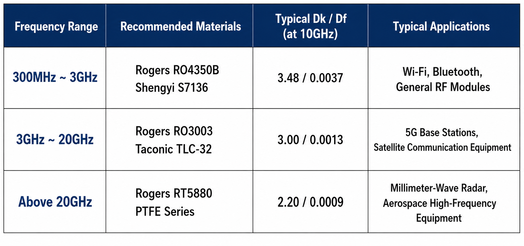
Core material-selection rule of thumb:
The higher the operating frequency, the lower the required Dk and Df of the material.
For cost-sensitive scenarios: give priority to high-quality domestic high-frequency substrates such as ShengYi and Huazheng;
For high-precision critical scenarios (5G/mm-wave/aerospace): recommend mature imported materials such as Rogers and Taconic.
4. Real-World Case Study
Project background: A customer's 5.8 GHz RFID antenna project initially used ordinary FR-4 material for prototyping.
Fault manifestation: Antenna gain was 3 dB lower than the simulated value, and actual communication distance was reduced by 50%.
Solution: Kinji's technical team intervened, replaced the substrate with Rogers RO4350B, and simultaneously re-matched the impedance parameters.
Final result: Antenna gain and communication distance both met the requirements, and the project passed acceptance in a single attempt.
Challenge 2: Loss of Characteristic Impedance Control — Parameter Deviation Exceeds Tolerance, Signal Integrity Fails
1. Problem Manifestation
The measured PCB impedance deviates from the design target by more than ±10%, causing severe signal reflection and worsening VSWR, externally manifested as insufficient receiver sensitivity, abnormal equipment communication, or even failure to establish a link.
2. Root Cause Analysis
High-frequency characteristic impedance (Z0) is jointly determined by dielectric thickness (H), dielectric constant (Dk), line width (W), line spacing (S), and copper thickness (T). Ordinary board manufacturers often control line-width tolerance only to about ±20%, but high-frequency signals are extremely sensitive to trace geometry:
A 10% line-width deviation ⟹ 5–8 Ω impedance shift.
At GHz frequencies, such an offset is enough to directly trigger signal integrity failure.
3. Solution
Design-side optimization:
Use professional high-frequency electromagnetic-field simulation tools such as Polar SI9000 or ADS for impedance pre-calculation and parameter sweeping;
Reserve 10%–15% parameter margin in the design to cover natural variations between material batches and during processing;
High-frequency critical traces should follow the "short, straight, and uniform" principle; sharp angles and right-angle routing are strictly prohibited to eliminate impedance discontinuity points.
Manufacturing-side control:
Kinji is equipped with precision exposure and vacuum etching equipment, achieving line-width control accuracy of ±0.02 mm and stable maximum impedance error within ±2%;
Each shipment is accompanied by a TDR impedance test report, ensuring data traceability.
4. Real-World Case Study
Project background: A customer's 7 GHz RF power divider project was previously prototyped at a conventional board manufacturer.
Fault manifestation: Center frequency shifted by as much as 300 MHz, and the function completely failed.
Solution: The project was transferred to Kinji, which implemented strict high-precision tolerance control during manufacturing (line width ±0.01 mm, dielectric thickness ±0.025 mm).
Final result: Impedance was stably locked at 50 ± 2.5 Ω, and frequency shift was compressed to within 50 MHz, with all indicators exceeding design expectations.
Challenge 3: Incorrect Surface Finish Selection — Poor Soldering Reliability and Abnormal Fluctuations in High-Frequency Loss
1. Problem Manifestation
PCB pads have insufficient solderability, with frequent cold joints and false soldering during SMT; or soldering appears intact, but measured high-frequency insertion loss is abnormally elevated, with poor batch-to-batch consistency, making mass production difficult.
2. Root Cause Analysis
High-frequency signal transmission exhibits a significant skin effect, with electromagnetic energy mainly concentrated in the extremely thin surface layer of the conductor. Therefore, the material, thickness, and flatness of the surface finish directly affect loss performance:
HASL: poor surface flatness, causing disordered high-frequency signal transmission paths and sharply increased loss;
ENIG: the nickel layer is magnetic and interferes with the high-frequency electromagnetic field distribution; additionally, nickel has relatively high resistivity, introducing extra skin-effect loss.
3. Solution
Targeted selection must be made based on operating frequency and component lead pitch:
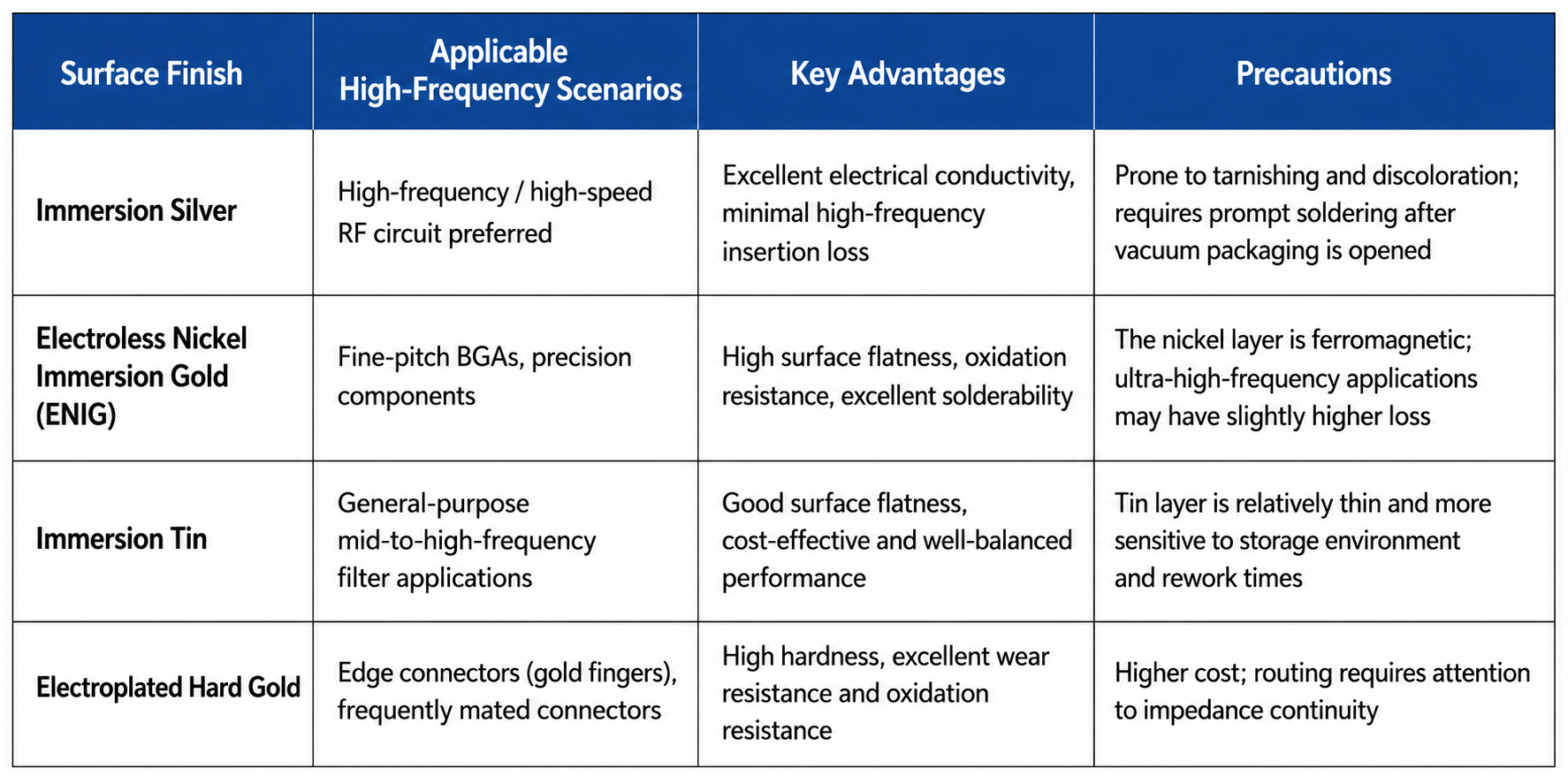
Golden rule for selection:
Pure RF/antenna circuits → immersion silver;
High-frequency boards with fine-pitch precision devices → immersion gold;
Plug-in contact structures → electroplated hard gold.
4. Real-World Case Study
Project background: An automotive 28 GHz millimeter-wave antenna project initially used conventional ENIG finish for prototyping.
Fault manifestation: The magnetic nickel layer introduced additional high-frequency insertion loss, and antenna gain was 1.5 dB lower than the simulated value, failing automotive-grade certification.
Solution: Kinji recommended changing the surface finish to immersion silver and re-prototyping.
Final result: The additional loss was completely eliminated, antenna gain recovered to the design standard, and the product successfully passed stringent automotive tests.
Challenge 4: Defects in High-Frequency Hybrid Lamination — Layer-to-Layer Misalignment, Compromising Overall Stability
1. Problem Manifestation
In multilayer boards using hybrid lamination of Rogers/PTFE high-frequency materials and FR-4, layer-to-layer misalignment, uneven dielectric thickness, and even delamination or blow-up after reflow soldering are highly likely, leading to total batch scrap.
2. Root Cause Analysis
High-frequency materials (especially PTFE resin systems) and FR-4 differ significantly in CTE and elastic modulus. During lamination:
The differing expansion and shrinkage characteristics of the two materials cause thermal stress concentration, leading to interlayer slippage and board warpage;
PTFE materials are soft and have poor flowability; conventional lamination processes tend to generate micro-voids, degrading dielectric layer thickness uniformity.
3. Solution
Design-side optimization:
adopt symmetrical stack-up structures to balance asymmetric thermal stresses during hybrid lamination; reserve sufficient compensation margins for alignment targets in multilayer boards.
Manufacturing-side control:
Kinji uses customized stepwise lamination processes (segmented temperature rise curves and pressure compensation mechanisms), first setting the high-frequency core layers and then laminating the FR-4 layers, effectively avoiding slippage caused by differential expansion and shrinkage;
High-precision alignment control stably keeps interlayer tolerance in hybrid boards within ±75 μm, completely eliminating delamination, voids, and warpage;
Each shipment includes a metallographic cross-section analysis report to quantitatively verify lamination quality and alignment accuracy.
4. Real-World Case Study
Project background: A customer's 4-layer RO3003 + FR-4 hybrid multilayer board project.
Fault manifestation: Initial prototyping through another channel showed layer misalignment exceeding 150 μm, causing severe distortion of the antenna radiation pattern.
Solution: Kinji optimized the stepwise lamination process and reduced layer misalignment to within 50 μm.
Final result: The symmetry of the antenna radiation pattern was fully restored, and the hybrid multilayer board met the reliability standards for mass production.
Challenge 5: Excessive Copper Foil Roughness — Hidden Transmission Loss, Causing Significant Deviation Between Measurement and Simulation
1. Problem Manifestation
The measured insertion loss of the high-frequency board is 0.5–1 dB higher than the simulated value. Even after replacing with higher-grade materials and optimizing the routing topology, this hidden loss stubbornly persists.
2. Root Cause Analysis
When high-frequency electromagnetic waves propagate in a conductor, the penetration depth (skin depth δ) is extremely small, and current flows only in the very thin surface layer of the copper foil. If the copper foil surface roughness is too high, the high-frequency current is forced to travel along microscopic peaks and valleys, effectively lengthening the actual transmission path and causing conductor loss to multiply.
Conventional electrodeposited copper foil (ED) typically has RMS roughness of 2–3 μm, which introduces significant additional loss above 10 GHz.
3. Solution
In millimeter-wave high-frequency scenarios at 10 GHz and above: give priority to rolled annealed copper foil (RA) or ultra-low-profile electrodeposited copper foil (HVLP) with RMS roughness of 0.3–0.5 μm to reduce conductor loss at the material source;
Kinji supports various specifications of high-grade low-roughness copper foil from 0.5 oz to 1.0 oz, and can provide copper-foil micro-morphology and roughness test reports for design verification.
4. Real-World Case Study
Project background: A customer's 77 GHz automotive millimeter-wave radar antenna project had a simulated insertion loss of 0.8 dB.
Fault manifestation: The initial prototype used conventional electrodeposited copper foil with 2.5 μm roughness, and the measured insertion loss reached 1.6 dB, causing radar ranging performance to fall short.
Solution: Kinji recommended replacing it with 0.4 μm ultra-low-roughness rolled annealed copper foil (RA).
Final result: Measured insertion loss dropped to 0.9 dB, closely matching the theoretical simulation, and the product successfully passed extreme automotive operating-condition tests.
Summary: Core Pitfall-Avoidance Guide for High-Frequency PCB Prototyping
The performance gap in high-frequency PCBs stems not only from routing layout but also from micro-level control of materials, tolerances, and processes. The following is a pitfall-avoidance reference for key areas:
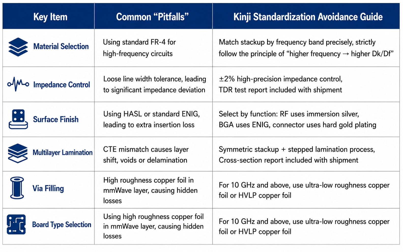
High-frequency and millimeter-wave circuits are highly sensitive to substrate parameters, copper foil physical properties, lamination precision, and surface finish. Kinji can now perform precision processing of 4- to 24-layer high-frequency boards, comprehensively covering special-process products such as 6 GHz–70 GHz high-frequency boards, millimeter-wave antenna boards, and ceramic/PTFE-based high-frequency boards, providing full-process technical support from prototyping to mass production for cutting-edge R&D projects.
Frequently Asked Questions About High-Frequency PCB Prototyping (Industry Hot Topics)
Q1: Can ordinary FR-4 material be used directly as a substitute for high-frequency PCBs?
Not recommended; substitution is strictly prohibited in the GHz band. Ordinary FR-4 materials have relatively high Dk and Df parameters and poor high-frequency stability. At frequencies below 300 MHz, they may be temporarily used in low-frequency scenarios, but at 3 GHz, 5G, and millimeter-wave frequencies, they will cause sharp increases in signal insertion loss, shortened communication distance, impedance drift, and other issues, directly resulting in substandard overall equipment performance. This is also the primary cause of high-frequency prototyping failure, so dedicated high-frequency substrates must be matched according to frequency.
Q2: What impedance deviation range is considered acceptable for high-frequency boards? Is a special test report required?
For ordinary PCBs, impedance tolerance of ±10% is acceptable, but the precision industry standard for high-frequency PCBs is ±2% to ±5%. GHz high-frequency circuits are highly sensitive to impedance; excessive deviation can cause signal reflection, standing-wave anomalies, and functional failure. Formal high-frequency prototyping must include a TDR impedance test report to ensure that the physical parameters are consistent with the simulation design, supporting R&D verification and production traceability.
Q3: For high-frequency RF circuits, should immersion gold or immersion silver be chosen?
The core depends on the circuit application: for pure RF signal transmission circuits, immersion silver is preferred because it offers the lowest high-frequency loss and best signal consistency; for high-frequency boards with BGA fine-pitch packaging and requiring multiple reflow soldering cycles, immersion gold should be chosen to ensure solderability; for frequently plugged gold-finger contacts, electroplated hard gold should be used. In high-frequency scenarios, HASL and ordinary OSP finishes should be avoided as much as possible.
Q4: Why are high-low-frequency hybrid boards prone to misalignment, blistering, and delamination? How can this be thoroughly resolved?
The core reason is the large difference in CTE between Rogers/PTFE high-frequency materials and FR-4 materials. Under high-temperature lamination, their expansion and shrinkage are not synchronized, and conventional one-step lamination readily causes misalignment, blistering, and delamination. The optimal solution is symmetric stack-up design combined with a customized stepwise lamination process: first set the high-frequency core layers, then laminate the ordinary substrate layers, which can control interlayer tolerance within ±75 μm and completely eliminate process defects.
Q5: If the insertion loss of a millimeter-wave high-frequency board does not match the simulation, what is most likely the problem?
After excluding material, routing, and impedance issues, 90% of the time it is due to excessive copper foil roughness. In millimeter-wave scenarios above 10 GHz, ordinary electrodeposited copper foil with high roughness generates substantial hidden additional loss through the high-frequency skin effect, causing measured insertion loss to be far higher than simulation. Replacing it with ultra-low-roughness rolled annealed copper foil or HVLP copper foil with RMS roughness of 0.3–0.5 μm can bring measured data into close agreement with simulation.
Q6: How can the first-article yield of high-frequency PCB prototyping be quickly improved?
Focus on five core points: precise material selection according to the operating frequency gradient, full-range high-precision impedance control, dedicated surface finishes for high-frequency scenarios, symmetrical stack-up with stepwise lamination, and millimeter-wave-grade low-roughness copper foil selection. At the same time, engage with the board manufacturer in advance to align simulation parameters, process requirements, and test standards, avoiding the conventional logic of general-purpose PCB manufacturing, which can greatly reduce rework rates and shorten the R&D cycle.
trending news
Contact Us