





Sorry, no sales person is available right now to take your call. Pls leave a message and we will reply to you via email as soon as possible.
Full Analysis of PCB Embedded Component Technology: Advantages and Applications
2026-07-22
Driven by the trends of lighter and thinner consumer electronics, higher-frequency communication equipment, and more reliable automotive electronics, traditional PCB Surface Mount Technology (SMT) faces three major challenges: "insufficient space, signal attenuation, and reliability bottlenecks." As products like smartphones, wearables, and 5G base stations push the physical limits of integration density, an innovative technology that can "hide" components inside the PCB—PCB Embedded Component Technology—is gradually becoming the core solution for high-end electronics manufacturing.
Kinji is a professional high-end PCB manufacturer with years of R&D and mass-production experience in advanced circuit substrates. We deliver one-stop custom PCB solutions covering embedded component boards, HDI, multi-layer high-density boards and ceramic substrates for global clients across consumer electronics, telecommunications, automotive, industrial control, medical devices and aerospace sectors. This article fully deconstructs the core value, practical application cases and key manufacturing specifications of embedded PCB technology to demonstrate how this advanced process reshapes electronic product design and manufacturing.
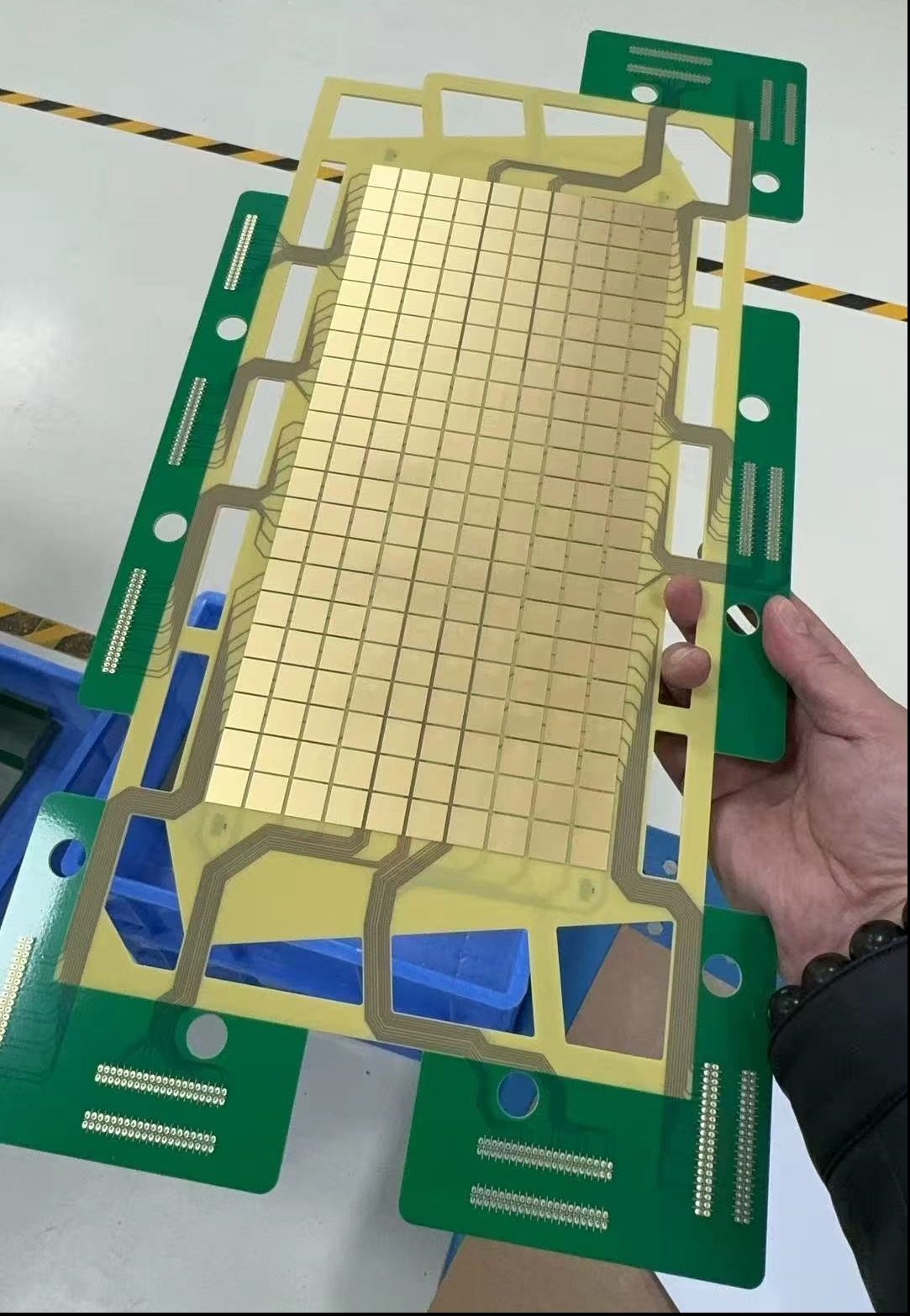
Kinji Embedded Component PCB Products
I. What is PCB Embedded Component Technology? Breaking the "Surface Mount" Mindset
Simply put, PCB embedded component technology involves embedding passive components such as resistors, capacitors, and inductors, and even active components like diodes and microchips, directly into the PCB substrate material. This is achieved through processes like routing cavities, precise placement, and lamination encapsulation, rather than mounting them on the board's surface. Electrical connections to the external circuits are made via inner-layer micro-blind vias and buried vias, forming an integrated "component-substrate-circuit" structure.
Compared to traditional processes, this "embedded" design completely transcends the limitations of "surface space competition." It no longer requires reserving large surface areas for SMD components and eliminates performance losses caused by long leads. This opens up new possibilities for the miniaturization and high-performance upgrading of electronic products.
II. Embedded vs. Traditional Processes: 5 Core Advantages Reshaping Product Competitiveness
1. Ultimate Space Optimization, Enabling Product "Slimming"
Traditional PCBs have significant surface area occupied by numerous SMD components, often preventing board size reduction or forcing compromises in functional integration. The embedded process can free up 20%-30% of the surface space, reducing the overall PCB area by 15%-25%. For size-sensitive products like smartwatches, wireless earbuds, and implantable medical devices, this is almost a "critical" requirement. For instance, using embedded resistors and capacitors on a smartwatch's main control board can free up space for a larger battery or more complex sensor modules.
2. Enhanced High-Frequency/High-Speed Performance, Suited for the 5G/mmWave Era
With the proliferation of 5G communications, automotive radar, and RF modules, signal integrity has become a critical success factor. In traditional processes, components connect to circuits via long leads, which can introduce parasitic inductance and capacitance, leading to high-frequency signal attenuation and severe crosstalk.
The embedded process directly interconnects components with inner-layer circuits, reducing connection paths from millimeters to micrometers. This significantly lowers parasitic parameters, reduces signal delay by over 30%, and markedly improves Electromagnetic Interference (EMI) suppression. This is precisely why overseas manufacturers of 5G base station equipment and high-end RF modules increasingly favor embedded technology.
3. Doubled Reliability, Suited for Harsh Application Environments
For clients in automotive electronics, industrial control, and aerospace, PCB reliability is directly linked to product safety and lifespan. Traditional SMD components rely on solder joints for fixation and connection, which are prone to cracking or detachment under harsh conditions like vibration, shock, and thermal cycling.
In the embedded process, components are completely encapsulated by the PCB resin substrate, providing a "natural protective layer." This shields them from dust, moisture, chemical corrosion, and buffers mechanical stress. Solder joint count is reduced by over 40%, significantly lowering product failure rates. Testing data from Kinji shows that PCBs for automotive ADAS modules using embedded technology have a lifespan more than twice as long as those using traditional processes in -40°C to 125°C thermal cycling tests.
4. Improved Thermal Management, Solving Heat Dissipation Issues for Power Devices
Heat dissipation in power devices and highly integrated modules is a persistent challenge in electronic design. In traditional processes, heat from surface components must conduct through surface pads to the substrate, offering a limited thermal path and creating localized hot spots. Embedded components are positioned closer to the PCB's inner layers, shortening the vertical heat dissipation path. Combined with high-thermal-conductivity prepreg materials, inner-layer copper foils, and metallized thermal vias, a multi-dimensional thermal path can be established to accelerate heat spreading and mitigate localized overheating.
5. Simplified Assembly Process, Balancing Overall Cost
While some clients worry about the cost of embedded technology, looking at the entire process reveals that it can offset costs by simplifying subsequent assembly steps. It reduces the number of components placed via SMT, shortens pick-and-place and reflow soldering processes, and lowers the consumption of placement fixtures and auxiliaries. Furthermore, reduced product size leads to lower shipping and storage costs. For high-volume production of high-end products, the total cost advantages of embedded technology become increasingly apparent.
III. What Scenarios are Best Suited for Embedded Technology? Precisely Matching Customer Needs
Embedded technology isn't a universal solution, but its core value of "miniaturization, high reliability, and superior performance" has been well-verified across six major overseas application scenarios, including consumer electronics and automotive electronics. Below, combined with real-world industry case studies and quantitative results, let's explore how embedded technology directly addresses key customer pain points and empowers product innovation.

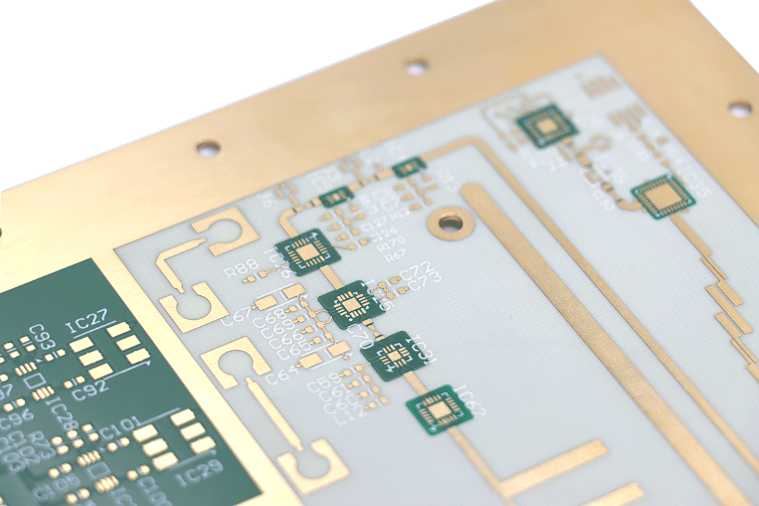
· Consumer Electronics: A Dual Breakthrough in Ultimate Thinness and High-Frequency Transmission
Core Pain Point: Smart wearables, foldable phones, etc., have stringent requirements for PCB size and thickness, while also needing stable high-frequency signal transmission.
Case Study: A leading global smartwatch brand needed to integrate 20+ passive components and an RF module on a 1.2mm thick main board for its next-gen product. Traditional SMT faced space limitations on the surface. By using Kinji's embedded technology, 15 passive components (resistors, capacitors) were embedded within the substrate, freeing up 30% of surface space. This resulted in a PCB thickness reduction to 0.8mm and a 25% reduction in RF signal transmission delay, meeting Bluetooth 5.3 high-frequency requirements. The product's battery life improved by 12% due to space for a larger battery. Additionally, a leading Chinese foldable phone manufacturer used embedded technology for the PCB in the hinge area, embedding microchips and inductors to solve the problem of components detaching after 200,000 bend cycles, improving reliability by 60%.
· Communication Equipment: Guaranteeing Signal Integrity in 5G/mmWave Scenarios
Core Pain Point: 5G base stations and RF modules need to address high-frequency signal attenuation, EMI interference, and high-density integration.
Case Study: A European 5G equipment manufacturer's 77GHz automotive radar module faced signal insertion loss exceeding 0.5dB/inch at 10GHz due to long component leads in traditional PCBs, failing to meet detection accuracy requirements. By embedding RF inductors and capacitors, the connection path was shortened from millimeters to micrometers, reducing parasitic inductance by 40%. Ultimately, the signal insertion loss was controlled below 0.18dB/inch, improving radar detection accuracy to ±0.1°, perfectly suited for autonomous driving sensing needs.
· Automotive Electronics: Achieving High Reliability under Harsh Conditions
Core Pain Point: ADAS systems and EV power modules must withstand harsh environments like thermal cycling, vibration, and shock; traditional SMD solder joints are prone to failure.
Case Study: A global Tier 1 automotive electronics supplier faced an 8% failure rate in traditional SMT solder joints during -40°C to 125°C thermal cycling tests on an ADAS domain controller PCB, failing to meet ISO 26262 functional safety standards. Using embedded technology, the core power devices and 12 resistors were embedded, reducing solder joints by 45%. Kinji reliability tests confirmed a failure rate below 0.5% after 500 thermal cycles, extending the lifespan by more than double compared to traditional processes. This technology is now used in batches for customers like Tesla and XPeng. In another instance, a new energy vehicle inverter utilizing chip-embedded PCB technology achieved stray inductance below 1nH, reducing switching losses by 30%, perfectly meeting 800V high-voltage platform requirements.
· Industrial Control: Ensuring Long-Term Stable Operation in Complex Environments
Core Pain Point: Industrial robots and PLC equipment need long-term reliable operation in dusty, vibrating, and wide-temperature environments; PCB reliability directly impacts downtime costs.
Case Study: A German industrial robot manufacturer faced frequent detachment of traditional SMD resistors under high-frequency vibration in their joint controller PCBs, costing over €1 million annually in maintenance. By embedding critical resistors and capacitors, these components were fully encapsulated by resin, passing IP67 protection level tests. They operated for 10,000 hours without failure under 2000Hz vibration, reducing maintenance costs by 90%.
· Medical Devices: Balancing Miniaturization and Biocompatibility
Core Pain Point: Portable diagnostic instruments and implantable devices require a balance of PCB miniaturization, biocompatibility, and high reliability.
Case Study: An overseas medical device company's portable ultrasound diagnostic device needed the PCB integrated into a palm-sized probe while meeting ISO 13485 biocompatibility certification. Using embedded technology, the signal processing chip and passive components were embedded, reducing PCB area by 25%. Using halogen-free substrates and OSP protective coating, it withstood 288°C for 10 seconds, fully complying with the stringent requirements of medical devices, while probe battery life increased by 20%.
· Aerospace: Meeting Demands for Lightweighting and Radiation Resistance
Core Pain Point: Satellite communication and drone systems require very high levels of PCB lightweighting, radiation resistance, and integration.
Case Study: An overseas drone manufacturer's airborne communication module faced weight issues with traditional densely populated PCBs, impacting flight time. By adopting an embedded component technology combined with a ceramic substrate solution, core circuits and passive components were embedded, reducing PCB weight by 18%. It also passed radiation resistance tests (Total Ionizing Dose of 100krad), improving signal transmission stability by 35% in high-altitude, low-pressure environments, meeting aerospace application standards.
IV. Implementing Embedded Component Technology: From Case Pain Points to Technical Solutions

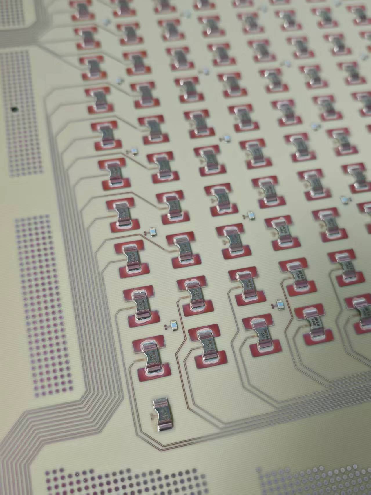
The implementation of embedded component technology places high demands on the PCB manufacturer's technical capabilities. The core challenges lie in four areas: "component alignment accuracy, lamination process control, interconnection reliability, and testing/inspection." As a manufacturer focused on high-end PCBs, Kinji leverages the following technical expertise to provide stable embedded technology solutions:
· High-Precision Placement: Uses laser marking of fiducial points and machine vision positioning to achieve component alignment accuracy within ±5μm, suitable for embedding miniature components.
· Optimized Lamination Process: Utilizes customized vacuum lamination profiles with stepwise heating and pressurization to prevent voids and uneven resin flow during lamination, ensuring tight component encapsulation.
· Reliable Interconnection: Employs laser drilling and plasma desmear techniques for precise micro-via depth control, combined with electroless copper plating to enhance adhesion strength and ensure stable inner-layer interconnections.
· Comprehensive Testing: Integrates multiple inspection methods, including X-ray inspection, AOI, and resistance/capacitance value testing, to preemptively mitigate batch risks.
V. Future Outlook: Embedded Technology Becoming Mainstream in High-End PCBs
As electronic product integration density continues to rise, the conflict between "space" and "performance" will intensify. Embedded component technology, as a core solution to this conflict, is moving from niche high-end applications towards the mainstream market. In the future, combined with technologies like 3D embedding, heterogeneous integration, and AI-assisted design, embedded technology will enable more complex component integration and optimized performance, providing even stronger support for customer product innovation.
Kinji remains customer-centric, continuously investing in advanced PCB process R&D. We offer global customers one-stop solutions including embedded component technology, ceramic substrates, HDI boards, high-multilayer boards, and more, helping your products stand out in the global market.
Are you facing issues like space constraints or high-frequency performance degradation in your product designs? Feel free to leave a comment to discuss; we can provide professional process solutions for you!
trending news
Contact Us