





Sorry, no sales person is available right now to take your call. Pls leave a message and we will reply to you via email as soon as possible.
Kinji High‑Order HDI Motherboard for Laptops – Ultra‑Thin, High‑Density & Low‑Interference, Empowering High‑Performance Lightweight Notebooks
2026-07-01
Introduction
Ultra‑lightweight design, powerful computing performance, and high integration have become irreversible trends in the laptop industry. End devices impose stringent requirements on PCBs in terms of wiring density, signal integrity, and thickness control. Leveraging Kinji’s years of R&D and precision manufacturing experience in high‑order HDI circuit boards, we proudly launch our 10‑layer 2nd‑order HDI laptop motherboard. Equipped with customized full‑process craftsmanship and premium substrate materials, this product addresses core industry pain points including dense wiring constraints, high‑speed signal crosstalk, and insufficient structural strength of ultra‑thin boards, delivering stable and reliable underlying hardware solutions for business ultrabooks and creative laptops.
1. Premium IT‑170GT Substrate – Building a Foundation for Low‑Loss High‑Speed Transmission
This motherboard adopts IT‑170GT high‑Tg copper‑clad laminate as the core dielectric material – a customized material developed by Kinji to adapt to long‑duration high‑temperature operating conditions of laptops.
IT‑170GT features a glass transition temperature (Tg) of 170°C, offering vastly improved heat resistance compared with standard FR‑4 substrates. Under continuous high heat generated by CPUs and GPUs under full load, it effectively restrains thermal expansion and contraction of the board, eliminating layer misalignment and hole displacement in the 10‑layer stacked structure. Meanwhile, its low Dk/Df dielectric properties drastically cut signal attenuation during massive high‑speed data transmission, ensuring stable data exchange between processors, memory modules, and high‑speed Thunderbolt ports without lag or disconnection.
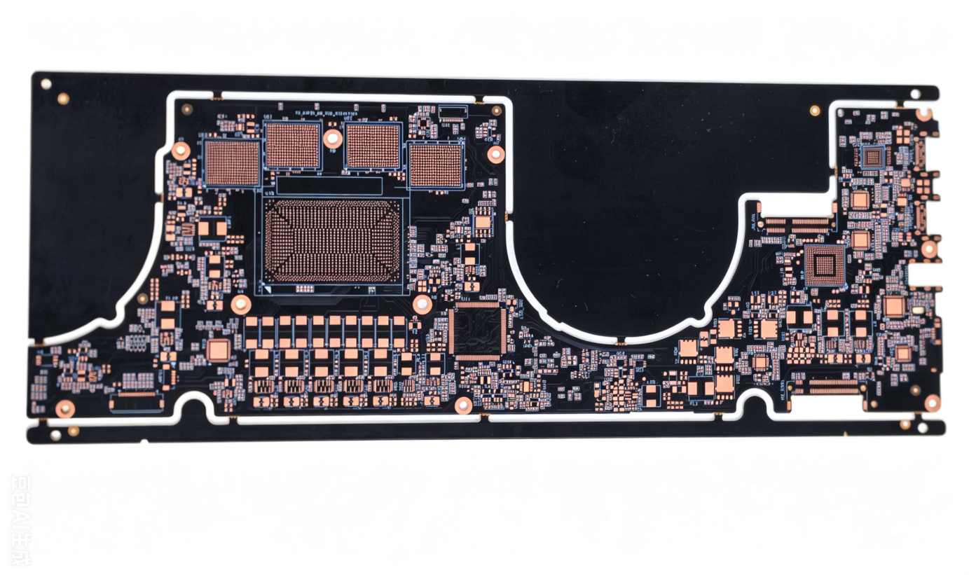
2. 10‑Layer 2nd‑Order HDI Stack‑up with 1.6mm Ultra‑Thin Thickness – Balancing Lightweight Form Factor & Computing Capacity
The core specification of the product is a 10‑layer 2nd‑order HDI structure, with finished board thickness precisely controlled at 1.6mm. It adopts a 1‑up standardized single‑panel production model, fully realized by Kinji’s automated precision production lines.
10‑layer stack‑up layout – Independently divided power planes, high‑speed signal layers, and ground shielding layers form multi‑layer shielding barriers to isolate high‑frequency electromagnetic crosstalk, perfectly supporting multi‑circuit power supply layout and high‑speed differential routing for mobile processors.
2nd‑order HDI blind & buried via technology – Superior interlayer connectivity over 1st‑order HDI, maximizing available surface routing space to accommodate more electronic components and interfaces.
1.6mm ultra‑thin board thickness – Kinji’s precision lamination technology with ultra‑thin prepregs minimizes overall board dimension even with stacked multi‑ounce copper foils, reserving more internal space for larger batteries and optimized heat dissipation channels to enable slimmer, lighter laptop chassis designs for OEMs.
1‑up single‑panel manufacturing – Independent processing and quality control for each single board avoids uneven lamination stress and pattern offset common in multi‑up panels, stabilizing mass production yield and supporting standardized bulk delivery of laptop motherboards.
3. Micron‑Level Microvia & Ultra‑Fine Wiring Technology – Maximizing Circuit Integration
Backed by Kinji’s core precision manufacturing processes including laser drilling and LDI (Laser Direct Imaging), the motherboard achieves industry‑leading microvia and routing precision, breaking layout limits of conventional PCBs with two core parameters:
Minimum finished via hole diameter: 0.2mm microvias
Our proprietary laser drilling production line forms tiny 0.2mm vias, combined with a hybrid blind/buried via interconnection design to drastically reduce the board area occupied by holes. High‑density interconnection is realized in compact zones around CPU chips and connectors, enabling placement of more resistors and capacitors within limited board space – the core process enabler for miniaturized, highly integrated laptops.
Ultra‑fine line width & spacing: 2.94mil / 2.94mil
Replacing traditional film exposure, LDI laser direct imaging delivers micron‑level pattern transfer accuracy, consistently producing equal‑width, equal‑spacing 2.94mil differential traces. For memory channels, wireless RF circuits, and Thunderbolt high‑speed interfaces, uniform traces maintain consistent impedance, reducing signal distortion and loss during high‑speed transmission to achieve low‑interference, high‑bandwidth data transfer.
Core Advantages & Application Value
Two Core Competitive Strengths:
Ultra‑thin board enables slimmer end devices – The 1.6mm 10‑layer thin stack paired with 2nd‑order HDI microvia layout cuts the footprint occupied by the motherboard inside the chassis. Brand OEMs can expand battery capacity and redesign cooling structures to deliver lighter notebooks with longer battery life.
Full‑system low‑interference high‑performance operation – The synergy of low‑loss IT‑170GT substrate, multi‑layer shielding stack‑up, and precision impedance‑controlled ultra‑fine traces greatly suppresses electromagnetic interference. Processors, high‑speed peripherals, and wireless modules run simultaneously under heavy load without thermal throttling or system lag.
Application Fields:
Kinji’s 10‑layer high‑order HDI laptop motherboard serves as the core hardware for high‑density integration in consumer electronics. It is widely applicable to premium business ultrabooks, graphic design laptops, and portable performance notebooks. Leveraging our fully in‑house controllable HDI precision manufacturing technology, we translate every precise process parameter into tangible end‑user performance benefits, helping consumer electronics brands launch benchmark notebooks combining sleek lightweight aesthetics and powerful computing capability.
Closing Remarks
As laptops continuously upgrade computing power while pursuing thinner form factors, high‑order HDI PCBs have become the core underlying technology driving differentiated competition for end products. Kinji maintains deep focus on R&D and manufacturing of high‑end precision circuit boards. With a complete set of advanced technologies including IT‑170GT premium substrates, 10‑layer 2nd‑order HDI ultra‑thin stack‑up, 0.2mm microvias, and 2.94mil ultra‑fine wiring, we deliver stable, cost‑effective high‑density motherboard solutions to laptop manufacturers worldwide, continuously advancing technological iteration for high‑density integration in consumer electronics.
trending news
Contact Us