





Sorry, no sales person is available right now to take your call. Pls leave a message and we will reply to you via email as soon as possible.
Piloting the 5G era: Kinji high-order HDI board builds the cornerstone of computing power interconnection with the ultimate technology
2026-07-01
With the evolution of 5G communication to high frequency, high speed and large capacity at full speed, the core communication equipment poses unprecedented severe challenges to the high integration of hardware carriers and the stability of signal transmission. As an industry pioneer in the field of high-end circuit board manufacturing, Kinji officially launched a 14-layer second-order HDI high-precision interconnection board tailored for 5G core communication modules.
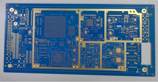
This product integrates Kinji's latest technological breakthroughs in the fields of micro blind hole drilling, precision graphics transfer and high-rise and multi-layer lamination, and interprets excellent quality with hard-core parameters, injecting strong power into a new generation of intelligent hardware and edge computing equipment.
I. In-depth analysis of core technical parameters: deconstructing the performance password of the ultimate process.
Relying on Kinji's mature high-end HDI manufacturing platform and strict quality control system, this 14-layer HDI board achieves a perfect balance between physical limit and electrical performance in a limited space:
14-layer second-order HDI structure & 1.70 mm fine plate thickness
In-depth interpretation: the second-order HDI structure means that the product has undergone multiple lamination and laser blind hole interconnection. Kinji perfectly accommodates 14 high-density circuits in 1.70 mm gold plate thickness through precise lamination alignment technology and shrinkage compensation algorithm. This not only greatly optimizes the wiring density in vertical space, but also provides a very short physical path for the high-speed transmission of multi-channel parallel signals, effectively reducing parasitic capacitance and inductance.
0.1mm minimum aperture (Laser Via)
Deep interpretation: micropore is the core symbol of HDI board. Kinji adopts the top-notch CO₂/UV laser drilling equipment in the industry, and stably realizes the processing of 0.08~0.1mm micro-hole blind holes. With the advanced Copper Filling process, the copper layer in the hole is ensured to be uniform and void-free, which greatly improves the fan-out ability of BGA pin-intensive areas and perfectly adapts to a new generation of 5G baseband chips with high pin count and fine pitch.
3.54 mil/3.54 mil extreme line width line spacing
In-depth interpretation: In high-density wiring, the slight deviation of line width and line spacing will cause characteristic impedance distortion. Kinji relies on high-resolution LDI (direct laser imaging) technology and vacuum etching system to strictly control the line width spacing at 3.54 mil/3.54 mil. High-precision pattern transfer endows the conductor with a nearly vertical sidewall profile, which compresses the impedance control accuracy within 5% and ensures the "zero" distortion of high-speed differential signals during transmission.
Asymmetric/multilevel inner layer copper thickness (1/1/1/0.5/0.5/0.5/0.5/1/1/1 oz) and 1.0 oz outer layer finished copper thickness.
In-depth interpretation: This product adopts an extremely complicated multi-level inner and outer copper thickness configuration (inner core signal layer 0.5 oz, power supply/stratum 1 oz;; The outer layer finally finished with a copper thickness of 1.0 oz). Kinji has overcome the world-class problem of board Warpage caused by uneven copper thickness by superb laminated symmetry control and resin filling technology. The large copper thickness design ensures the efficient transmission and distribution of ultra-large current, while the fine inner layer of 0.5 oz takes into account the agile transmission of high-frequency signals.
Shengyi S1000-2M top-level high-frequency and high-speed plates
Deep interpretation: the substrate is the key to determine the signal attenuation. Kinji YEATION Shengyi S1000-2M professional plate with high Tg and low Dk/Df value. The material has excellent heat resistance and dimensional stability, and shows extremely low dielectric loss at 5G high frequency band, which can effectively resist the thermal shock caused by long-term high-power operation.
High standard gold sinking (ENIG) surface technology
In-depth interpretation: The top chemical nickel-gold (ENIG) surface treatment is adopted. The deposited gold layer is extremely flat, which provides excellent welding base for micro components, and has long-term oxidation and wear resistance, which perfectly avoids the risk of "black nickel" and ensures the contact resistance to be stable throughout the life cycle.
II. Core application scenario case: from parameter highlights to customer benefits
[Application Scenario] 5G Industrial Edge Computing Gateway
Parameter highlights: 3.54 mil fine line width and line spacing+0.1mm minimum aperture+S1000-2M high frequency substrate.
Pain point of the corresponding scene: Under the harsh working conditions of smart factories, fully automated production lines require edge computing gateways to simultaneously process high-speed video streams of multi-channel 4K ultra-high-definition industrial cameras in a very small volume, and there is strong electromagnetic interference and continuous high temperature (up to 85°C) at the scene. Due to the high frequency loss and poor signal isolation of traditional PCB, it is easy to cause data packet loss, equipment crash and production line shutdown.
Product solution: Kinji 14-layer second-order HDI board is introduced. Its precise impedance wiring of 3.54 mil and the ultra-low dielectric loss of S1000-2M construct a signal transmission channel with high bandwidth and low delay. The micro blind hole design of 0.1mm greatly shortens the interconnection distance between layers and forms a natural electromagnetic shielding effect.
Customer benefits: The gateway can run stably all day in harsh industrial sites, with the data transmission packet loss rate directly reduced to zero, and the heat dissipation efficiency increased by 25%, which greatly improved the comprehensive efficiency (OEE) of enterprise production line.
III. Conclusion
Every micron of progress is a manifestation of technical precipitation. Kinji 14-layer 2-order HDI board is not only a circuit board carrying components, but also the technological crystallization of Kinji's dialogue with the future through craftsmanship. From strict physical parameters to surging scene performance, Kinji has always been committed to providing the most reliable interconnection solutions for global hard technology innovators.
Kinji, make the interconnection more accurate and the future more efficient.
trending news
Contact Us