
Sorry, no sales person is available right now to take your call. Pls leave a message and we will reply to you via email as soon as possible.
High Density Interconnect (HDI) PCB | High-precision Circuit Board for Intelligent Electronics & Edge Computing
2026-06-15
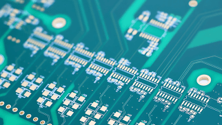
Fueled by the rapid development of edge computing, high-speed communication and smart electronic technology, modern intelligent devices are evolving toward ultra-miniaturization, high-density integration and high-frequency high-speed operation. Traditional PCBs can hardly meet the stringent requirements of compact circuit layout, precise signal transmission and structural stability, restricting the performance upgrade of high-end electronic equipment. As a professional high-precision PCB manufacturer, Kinji high-density interconnect (HDI) PCBs leverage advanced micro-processing technology to solve core industry pain points, delivering high-yield, high-stability and customizable circuit solutions for precision intelligent electronic scenarios.
Industrial-Grade Precision Core Specifications
Kinji HDI PCBs adopt a full set of industrial-grade precision parameters, achieving an optimal balance of ultra-fine wiring capability, high-frequency signal stability and mechanical reliability to adapt to high-end consumer and industrial electronic applications.
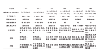
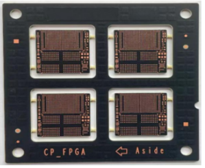
Equipped with leading micro-processing capacity, our HDI boards support 25μm/25μm minimum line width and space and 75μm minimum laser blind hole diameter. Empowered by Kinji’s laser direct imaging and precision laser drilling technology, it realizes consistent micron-level circuit patterning and dense layer interconnection, significantly boosting board space utilization and supporting ultra-thin, highly integrated product design. Customizable 2–12 layer structures with first-order, second-order and high-order blind & buried hole stacking fully meet diverse high-density layout requirements.
For high-frequency operating scenarios, the product features a stable DK value of 3.2–3.8 @1GHz, effectively reducing high-frequency signal attenuation and distortion. Optional 12μm–70μm copper foil thickness flexibly adapts to precision signal circuits and power supply circuits. Supported by ±5% strict impedance tolerance control, it maintains excellent signal integrity during high-speed operation. The ≤0.7% board warpage ensures superior flatness for fully automatic SMT mass production.
Multiple surface finishes are available, including immersion gold, immersion silver, OSP, solder paste and hard gold, catering to different assembly processes and complex service environments. All products are certified by RoHS, UL and IPC-A-600, fully complying with global industrial quality and environmental standards.
Kinji Empowered Core Technical Advantages
Relying independently optimized micro-fabrication and lamination processes, Kinji HDI PCBs possess exclusive technical strengths to break through the manufacturing limitations of traditional precision circuit boards.
Ultra-fine & high-density wiring. Advanced laser direct imaging and precise micro-etching technology enable stable micron-level circuit formation, maximizing wiring density and realizing compact circuit layout without compromising electrical performance, perfectly fitting miniaturized device design trends.
High-precision layer interconnection. High-accuracy laser drilling ensures complete, smooth hole walls and ultra-low conduction resistance. It shortens signal transmission paths, reduces transmission delay, and guarantees efficient and stable data transmission for high-speed computing and communication systems.
Excellent high-frequency signal stability. Matched with high-stability dielectric substrates and full-process impedance calibration, the board effectively suppresses signal crosstalk, attenuation and waveform distortion, maintaining reliable signal integrity under long-term high-frequency working conditions.
Superior structural reliability. Optimized multi-stage lamination and stress relief processes eliminate internal board stress, strictly controlling warpage issues. Excellent flatness prevents soldering deviation and virtual welding defects, fully adapting to high-efficiency automatic SMT production lines.
Highly flexible customized solutions. Diversified copper thickness options and rich surface finish processes support personalized customization for signal circuits, power circuits and various harsh application scenarios, covering multi-industry precision application demands.
Core Application Scenarios
Thanks to ultra-high precision, high integration density and outstanding high-frequency stability, Kinji HDI PCBs are widely used in smart wearable devices, industrial edge computing gateways, automotive electronics, high-speed communication modules, intelligent hardware, industrial main control boards and high-precision electronic equipment, providing solid and reliable core circuit support for miniaturized, high-speed and high-reliability intelligent terminals.
Breakthroughs in HDI Manufacturing Bottlenecks
High-end HDI PCB manufacturing faces prominent technical thresholds: ultra-fine wiring requires ultra-precise etching to avoid open/short circuits; multi-layer blind and buried hole stacking demands extreme alignment accuracy; repeated lamination processes easily cause stress concentration and excessive warpage; high-frequency impedance matching requires professional simulation and full-process verification.
As a certified Specialized, Refined, Unique & Innovative PCB manufacturer, Kinji tackles these industry bottlenecks via refined process control, high-precision optical alignment, professional stress optimization and full-link impedance testing, ensuring stable quality and high yield for mass production.
One-Stop Customization & Mass Production Service
Kinji provides full-lifecycle professional services including free DFM review, fast prototype sampling and stable volume production. With rich high-end HDI manufacturing experience, we deliver high-quality, compliant PCB products for various precision intelligent and industrial electronic projects.
Submit your Gerber files via our official website www.kinjipcb.com to get tailored technical solutions and exclusive quotations.
trending news
Contact Us