

Sorry, no sales person is available right now to take your call. Pls leave a message and we will reply to you via email as soon as possible.
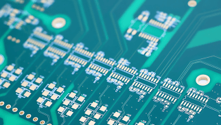
Custom Thick Copper PCB | High Current Heavy Copper Circuit Board for New Energy Power Industry
2026-06-15
Driven by the rapid upgrading of new energy and high-power power electronics, modern charging, photovoltaic and industrial control systems are raising unprecedented requirements for high-current load capacity, efficient thermal dissipation and long-term operational reliability. Standard PCBs can hardly withstand extreme high-power working conditions, resulting in insufficient current carrying, excessive heat accumulation and poor structural stability in heavy-load scenarios. As a high-end customized solution for power-grade circuits, Kinji thick copper PCB empowers high-power equipment with precise specifications and optimized manufacturing processes, effectively resolving core pain points in new energy power applications.
Precision Specification Design | Industrial-Grade Parameters for High-Power Scenarios
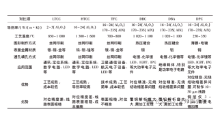
Every technical parameter of Kinji heavy copper PCB is professionally calibrated for high-current power scenarios, delivering stable, repeatable and industrial-grade performance.
6oz customizable inner and outer copper weight: Copper weight determines a PCB’s maximum current conduction capability. Supported by Kinji’s precise copper foil lamination and uniform thickness control technology, the optional 6oz heavy copper structure greatly expands the conductive cross-section of circuit traces, enabling reliable transmission of ultra-large current and laying a solid foundation for high-load power operation.
8-layer multilayer structure & 2.4mm finished board thickness: The mature 8-layer layered design realizes independent partitioning of power layers, signal layers and ground layers, isolating high-power circuits from weak-current signal circuits to avoid electromagnetic interference and improve system stability. The optimized 2.4mm board thickness balances structural rigidity and heat conduction efficiency, perfectly matching the assembly and heat dissipation design of industrial high-power equipment.
Ultra-high machining precision: Kinji achieves ±0.1mm dimensional tolerance and ≤±8% copper thickness tolerance through advanced precision etching and molding processes. Strict dimensional tolerance ensures accurate equipment assembly and seamless structural matching, while ultra-low copper thickness deviation eliminates local current imbalance and hotspots, ensuring consistent and stable current delivery across the entire board.
Authoritative industry certification: All products comply with RoHS, UL and IPC-A-600 standards, meeting global environmental and quality specifications for new energy, industrial control and smart grid equipment, supporting worldwide market access and large-scale commercial deployment.
Core Technical Advantages | Kinji Technology Empowers Performance Breakthroughs
Aiming at high current, high temperature and high reliability demands of the new energy power industry, Kinji optimizes lamination, electroplating and structural design, forming four exclusive core advantages.
1. Excellent high-current load capacity. Relying on Kinji’s mature heavy copper trace forming process, the extra-thick copper traces support extreme large-current conduction. The expanded conductive area effectively reduces circuit voltage drop and lowers operating heat generation, minimizing power loss and ensuring stable, continuous output under long-term heavy-load conditions.
2. Superior thermal dissipation performance. Kinji adopts a high-thermal-conductivity internal structure for thick copper PCBs, building an efficient heat dissipation channel that rapidly exports concentrated operating heat. This active heat dissipation mechanism prevents heat accumulation, avoids overheating failure of core power components, and greatly improves equipment durability in high-power operation.
3. Stable and reliable mechanical properties. Thick copper boards are prone to copper wrinkling, delamination and foil lifting during production and service. Kinji optimizes lamination pressure parameters and repeated electroplating processes to eliminate structural defects fundamentally. All products pass stringent thermal cycle reliability tests, maintaining stable internal structure and strong environmental adaptability under drastic temperature fluctuations and long-term continuous operation.
4. Diversified customized processing solutions. To adapt to the miniaturization and integration trend of power equipment, Kinji supports customized processes including plug hole, half-hole and embedded copper ingot processing. These flexible customization methods enable more compact power circuit layout, save internal equipment space, and support lightweight and integrated design of high-power terminal products.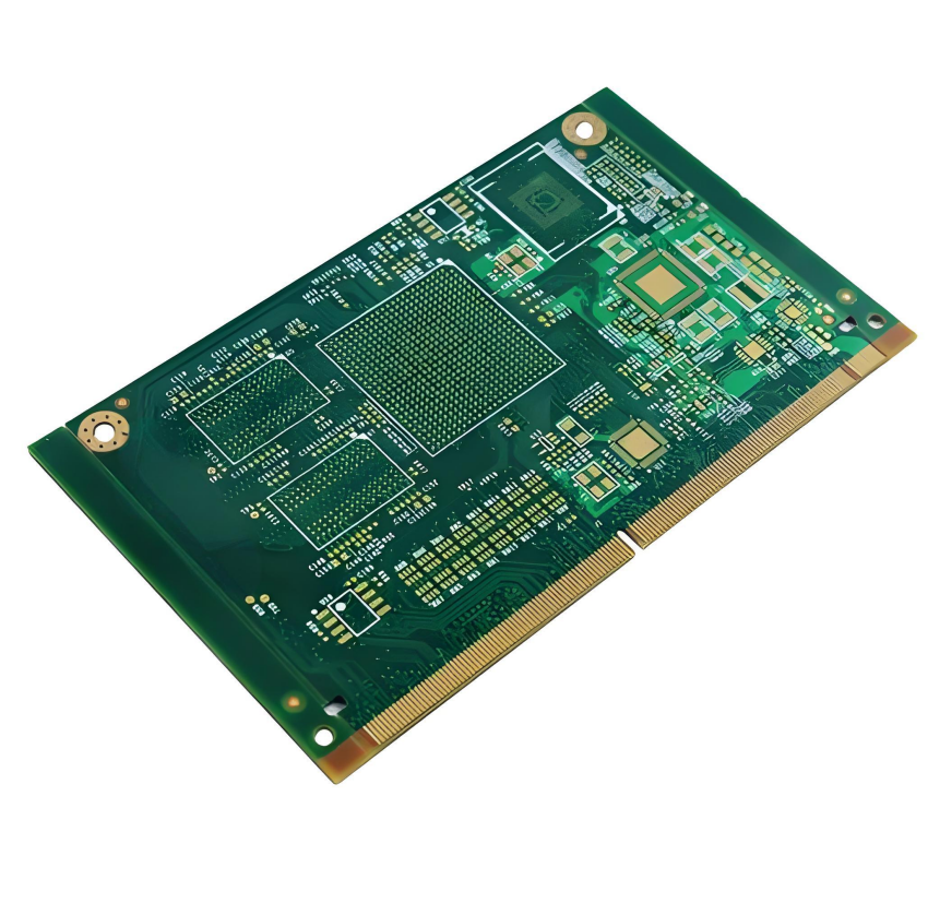
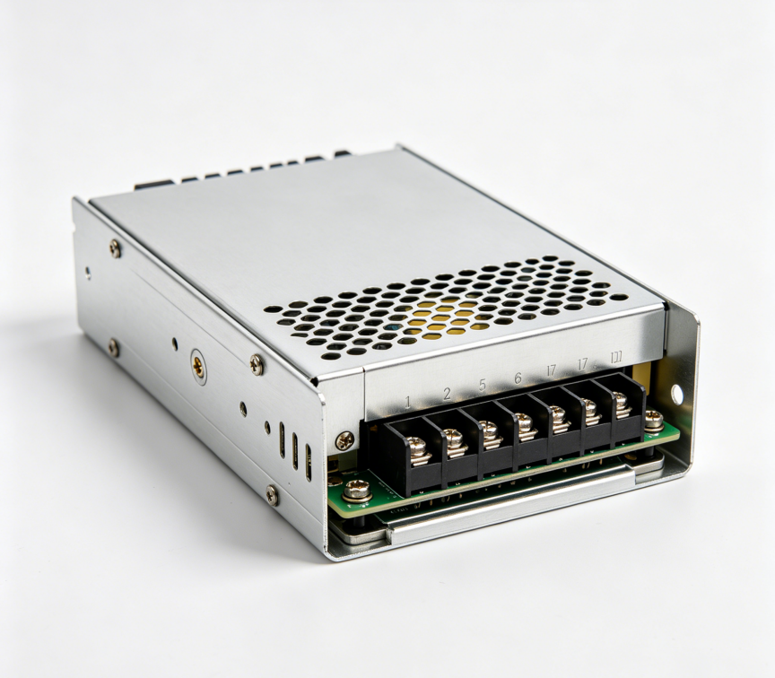
Wide Application Coverage | Serving Full-Scenario New Energy & Industrial Power Fields
Benefiting from high current resistance, efficient heat dissipation and high structural reliability, Kinji custom thick copper PCBs are widely applied in core high-power equipment, including new energy vehicle charging piles, solar inverters, industrial servo controllers, UPS uninterruptible power supplies, smart grid modules, as well as welding and automation power control equipment. It provides long-term stable circuit support for both outdoor new energy equipment and 24/7 continuous-running industrial control devices.
Break Through Manufacturing Barriers | Strict Process Control Ensures Consistent Quality
Heavy copper PCB manufacturing faces inherent industry challenges: thick copper foil leads to insufficient resin infiltration during lamination; thick copper etching easily causes open/short circuits; repeated electroplating requires ultra-precise parameter control for uniform board-wide copper thickness.
As an authoritative specialized, refined, unique and innovative PCB manufacturer, Kinji has overcome these key process bottlenecks. By optimizing lamination formulas and pressure curves, we solve poor resin infiltration of thick copper boards. The intelligent precise etching system eliminates circuit defects, and standardized electroplating parameter management guarantees consistent copper thickness across batches, achieving high consistency and high yield for mass production.
One-Stop Custom Service | Fast Sampling & Reliable Mass Production
Kinji focuses on the R&D and production of high-end power-grade thick copper PCBs. We provide full lifecycle services including free DFM review, rapid prototype sampling and stable volume production. From project evaluation and scheme optimization to proofing and batch delivery, we implement strict quality control at every step to meet personalized customization and high-standard quality requirements.
Submit your Gerber files via our official website www.kinjipcb.com to get a tailored solution and exclusive quotation for your thick copper PCB project.
trending news
Contact Us