
Sorry, no sales person is available right now to take your call. Pls leave a message and we will reply to you via email as soon as possible.
High-precision 12-Layer 3rd-Order HDI PCB | Empower Industrial Intelligent Hardware | Kinji CloudPCB
2026-06-02
Exquisite Craftsmanship, Zero Performance Weaknesses: Kinji CloudPCB’s 12-Layer 3rd-Order HDI Board Drives Core Industrial Intelligence
High-end industrial sectors—including industrial control, edge computing, precision testing, and industrial communication—impose stringent demands on equipment stability, integration density, and high-speed signal integrity. As the central interconnection carrier and structural backbone of intelligent industrial devices, high-density interconnect (HDI) PCBs largely determine the performance ceiling and service life of terminal equipment.
To address the growing need for miniaturization, high computing power, and long-term reliable operation in modern industrial systems, Kinji CloudPCB officially launches its 12-layer 3rd-order HDI PCB—a premium industrial HDI solution for high-end intelligent hardware. With advanced lamination technology and industrial-grade quality control, this HDI board breaks through the limitations of traditional PCBs, accelerating the iterative upgrade of high-performance industrial intelligent devices across diverse application scenarios.
🔧 Advanced Lamination Technology – Building a Solid Foundation for High-Density Interconnection
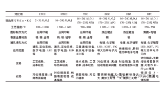
Our 12-layer 3rd-order HDI PCB adopts industry-leading third-order lamination technology combined with sophisticated blind and buried via structures, creating a high-reliability, low-loss, high-frequency HDI PCB. This innovative architecture overcomes the layout constraints of conventional printed circuit boards. Within an ultra-thin thickness of just 1.2 mm, 12 circuit layers achieve orderly hierarchical interconnection, effectively eliminating the stub effect during high-frequency signal transmission. The result is a low-loss, low-crosstalk, and highly consistent transmission channel that supports real-time high-speed data interaction for premium industrial hardware.
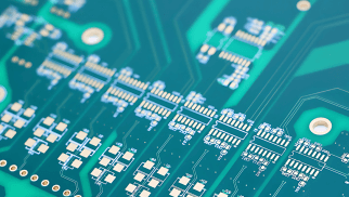
Micron-Level Fine Wiring for High-Density Packaging
Engineered with hairline-precision circuit patterning, this 0.2 mm micro-via HDI PCB supports a minimum hole size of 0.2 mm and features controlled line width/spacing of 2.95/3.54 mil. It is fully compatible with high-density packaged components such as BGA, QFN, and μBGA. The well-organized circuit layout effectively solves critical design challenges related to miniaturization and high integration, providing reliable technical support for the development of lightweight and highly integrated industrial devices.
Graded Copper Thickness Design for Balanced Performance
The inner layers adopt a differentiated copper thickness configuration of 1/1/0.5/0.5 oz, while the outer layers maintain a standard finished copper thickness of 1.0 oz. This scientifically optimized structure balances low-loss signal transmission with high-current load capacity. It not only ensures clean high-frequency signal transmission but also strengthens the current-carrying capability of power and ground layers. Additionally, the upgraded heat dissipation design enables continuous and stable operation under long-term high-load conditions.
🛡️ Premium Material Selection – Establishing Industrial-Grade Reliability Barriers
Industrial operating environments are often plagued by extreme temperature fluctuations, high humidity, dust accumulation, and frequent vibration. Material quality and mature manufacturing processes are prerequisites for long-lifespan industrial equipment. Adhering to strict industrial-grade manufacturing standards, Kinji CloudPCB controls every production step—from substrate selection to surface finishing—to enhance the environmental adaptability of this high-reliability industrial HDI circuit board and maximize operational reliability.
We select Shengyi S1000-2M, a high-performance industrial-grade substrate, as the core material for this premium industrial-grade 12-layer HDI board. With a high Tg value of 170 °C and an ultra-low coefficient of thermal expansion, the substrate effectively prevents deformation, delamination, and cracking caused by drastic temperature changes. The finished PCB offers excellent via stability and superior CAF (conductive anodic filament) resistance, delivering outstanding moisture resistance, aging resistance, and corrosion resistance for harsh industrial scenarios. As a lead-free FR-4 eco-friendly material, it complies with global environmental regulations and provides favorable mechanical processability, ensuring high yield and consistent quality during mass production.
The board surface features professional electroless gold plating (ENIG) , forming a dense nickel-gold composite protective layer—making it a stable electroless gold plating HDI PCB for industrial applications. On one hand, the ultra-flat surface completely avoids the dog-bone effect common to traditional hot-air leveling processes, creating an ideal soldering base for fine-pitch precision components and reducing defects such as cold or empty solder joints. On the other hand, the chemically inert gold layer provides exceptional oxidation and corrosion resistance for solder pads, extending the storage life of PCBs and the overall service life of intelligent industrial equipment.
🎯 Versatile Industrial Applications – Empowering Full-Scenario Intelligent Upgrades
Benefiting from high-density routing, exceptional stability, and strong scenario adaptability, Kinji CloudPCB’s 12-layer 3rd-order HDI board has been widely deployed across multiple high-end industrial fields. As a professional custom industrial HDI PCB manufacturer, we deliver core hardware components that boost the overall performance and quality of diversified intelligent industrial terminals.
Case 1: Core PCB for Embedded AI Vision Controllers
In collaboration with Zhiwei Industrial, our HDI board for AI vision controllers serves as the core signal interconnection carrier for the PAS-2310/6101 series embedded AI vision controllers. The 12-layer high-density hierarchical layout perfectly matches high-end computing platforms such as the RK3588 and NVIDIA Jetson AGX Orin. It enables low-latency, highly synchronized data interaction between computing units and peripheral interfaces. Supported by ultra-thin thickness and high integration, the vision controller achieves miniaturization, low power consumption, and cost-effectiveness. It has been widely applied in industrial visual inspection, intelligent quality detection, and automated sorting, with a signal error rate far below the industry average.
Case 2: CPU Core Board for Multi-Core Industrial Computers
Our 12-layer 3rd-order HDI PCB provides a one-stop solution to resolve bottlenecks in high-density wiring, high-current transmission, and heat dissipation for high-end multi-core industrial computers. This dedicated HDI PCB for industrial computers uses third-order lamination to achieve efficient interconnection between CPU cores and high-speed interfaces such as DDR and PCIe, while micron-level routing accuracy perfectly matches fine-pitch BGA packaging requirements. The graded copper thickness structure optimizes power and ground layer distribution, suppresses signal crosstalk, and enhances heat dissipation efficiency. It supports 7×24-hour uninterrupted high-load operation of industrial computers with powerful environmental adaptability.
Case 3: Backplane PCB for CPCI/PXI Precision Test & Measurement Devices
For high-end CPCI/PXI bus test and measurement equipment, our CPCI/PXI test equipment backplane PCB provides reliable backplane interconnection. The electroless gold plating process delivers superior soldering stability and wear resistance, adapting to frequent plugging and high-vibration working conditions while preventing loose connections on high-density connectors. Combined with the high-Tg substrate’s excellent thermal stability, the PCB maintains consistent bus signal transmission despite long-term temperature fluctuations, fully meeting the strict precision and repeatability standards of professional test and measurement equipment.
Beyond the above scenarios, this industrial HDI PCB is also suitable for edge computing gateway HDI PCBs and industrial communication module high-density PCBs, covering industrial tablets, intelligent measurement & control terminals, and more. It accelerates the miniaturization, integration, and high-performance upgrading of intelligent industrial devices worldwide.
💎 One-Stop Custom Service – Partner with Kinji to Win the Intelligent Future
With years of in-depth experience in high-precision industrial PCB R&D and manufacturing, Kinji CloudPCB adheres to the quality philosophy of Micron‑Level Precision, Industrial‑Grade Standard. As a reliable one-stop HDI PCB solution provider, we offer customized services covering solution optimization, process adaptation, prototype manufacturing, and mass delivery—balancing premium quality and efficient delivery for global clients.
Kinji CloudPCB’s 12-layer 3rd-order HDI PCB represents the perfect integration of advanced manufacturing technology, premium raw materials, and industrial scenario-oriented design. We polish every printed circuit board with ultimate craftsmanship to consolidate the performance foundation of intelligent industrial equipment.
Partner with Kinji for high-precision HDI PCBs to enhance your product competitiveness and jointly explore new opportunities in the global industrial intelligence era.
trending news
Contact Us