


Sorry, no sales person is available right now to take your call. Pls leave a message and we will reply to you via email as soon as possible.
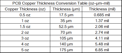
PCB Copper Thickness Conversion Table (oz–μm–mil) & 1oz Copper Thickness Explanation
2026-02-25
1. Core Question About 1oz Copper Thickness
In PCB production communication and specification sheets, we often hear "1oz copper thickness" and default that it corresponds to approximately 35 microns (μm). This seemingly regular value is not arbitrarily set, but a result of precise physical definitions, unit conversions, and industry practice conventions. The logic behind it is clearly explained from three aspects: definition, conversion, and engineering significance.
(1)True Definition of "1oz Copper Foil" (PCB Industry Standard)
In the PCB industry, "1oz copper foil" does not directly describe the thickness of the copper foil, but refers to a areal density standard: "the average thickness of a copper foil formed by uniformly laying 1 ounce (oz) of pure copper on an area of 1 square foot (1 ft²)". Simply put, it is essentially a combined definition of "weight + area", and the thickness is calculated inversely through this definition.
(2)Unit Conversion and Thickness Calculation (Key Steps)
To obtain the thickness corresponding to 1oz copper foil, it is necessary to first unify the units (convert from imperial to metric), then calculate using physical formulas. The specific steps are as follows:
- Core Conversion Steps for 1oz Copper Thickness (Top Priority)
- Step 1: Unify Units (Core Premise) 1 ounce (oz) = 28.35 grams (g) (Weight Unit Conversion)
- 1 square foot (ft²) = 929.03 square centimeters (cm²) (Area Unit Conversion)
- Density of copper ≈ 8.96 g/cm³ (Industry Universal Reference Value)
- From Mass (m) = Density (ρ) × Volume (V) and Volume (V) = Area (S) × Thickness (t), derive: Thickness (t) = Mass (m) ÷ (Density (ρ) × Area (S))
- t = 28.35 g ÷ (8.96 g/cm³ × 929.03 cm²) ≈ 0.00341 cm
- 0.00341 cm × 10000 = 34.1 μm (Theoretical Value), uniformly rounded to 35 μm (Standard Nominal Value) in the industry
- Step 2: Derive Thickness Formula
- Step 3: Substitute Values for Calculation
- Step 4: Unit Conversion and Industry Rounding
(3)Key Points and Engineering Significance (Must-Read)
- Why is weight used instead of direct thickness for definition? This is an industrial convention that has been followed in the PCB industry. The core reason is "easy measurement and easy control": the copper foil used in PCBs is extremely thin, and direct thickness measurement during online production is difficult and has high errors; while the weight (ounce) of copper foil can be controlled through precise weighing. Defining copper foil specifications based on this standard can be more efficiently applied to procurement, production management and quality inspection, ensuring the consistency of mass production.
- Why is there a deviation in actual thickness? The actual thickness of copper foil labeled 1oz is not fixed at 35μm, but usually fluctuates between 32-36μm. There are two main reasons:Manufacturing tolerance: Any industrial production has an allowable error range, and slight fluctuations in thickness during copper foil production are normal;Difference in copper foil types: Common copper foils are divided into rolled copper and electrolytic copper. The former has a denser and smoother structure, while the latter has relatively rough crystals. The two have slight differences in density and surface contour. Even if the nominal weight is the same, the actual average thickness will be slightly different.
- Key impact of copper thickness on PCB design Copper foil thickness is directly related to the performance and reliability of PCB, which should be focused on during design:Current carrying capacity: The thicker the copper foil, the larger the current that the conductor can safely pass, avoiding burnout due to overheating during long-term use;Impedance control: In high-frequency and high-speed circuits (such as USB, HDMI, radio frequency circuits), the characteristic impedance of the conductor is directly related to the copper thickness and its cross-sectional size. The copper thickness needs to be precisely controlled to ensure signal transmission quality;Heat dissipation performance: Thicker copper foil has higher thermal conductivity, which can help components (such as chips) on the PCB dissipate heat better and extend the service life of the product.
2. Excel Direct Copy Format (Auto-Generate Table After Pasting)
Note: Copy all the above lines and paste them directly into Excel. Excel will automatically recognize the tabs and generate a standard table without manual adjustment of column width.
trending news
Contact Us