

Sorry, no sales person is available right now to take your call. Pls leave a message and we will reply to you via email as soon as possible.
An In-depth Analysis of 5 Metallization Processes for PCB Ceramic Substrates: Principles, Performances, and Application Scenarios
2026-02-04
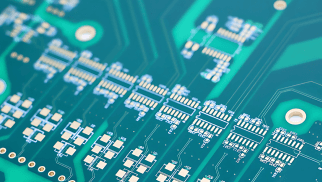
Ceramic substrates have become the cornerstone of high-power, high-density electronic packaging due to their excellent insulation, thermal conductivity, and mechanical stability. Metallization, the key process of forming conductive layers on ceramic surfaces, directly determines the electrical connectivity, thermal management, and long-term reliability of PCB ceramic substrates. Currently, the mainstream metallization methods include Direct Plated Copper (DPC), Thick Film Metallization (TFC), Direct Bonded Copper (DBC), Direct Bonded Aluminum (DBA), and Active Metal Brazing (AMB). This article will elaborate on the core principles, performance characteristics, advantages, disadvantages, and typical application scenarios of each process, providing valuable references for industry practitioners.
1. Direct Plated Copper (DPC): Low-Temp Metallization for Precision Optoelectronic Applications
DPC is a precision metallization technology that realizes copper layer deposition on ceramic surfaces through a two-step process: seed layer sputtering and electroplating accumulation. Specifically, it first uses Physical Vapor Deposition (PVD) technologies such as magnetron sputtering or vacuum evaporation to deposit a thin metal underlayer (seed layer) on the cleaned ceramic surface. This seed layer serves as a conductive base for subsequent electroplating, ensuring uniform growth of the copper layer. Then, the substrate is placed in an electroplating bath, and the copper layer is deposited to the predetermined thickness by controlling the electroplating current and time.
The most prominent advantage of DPC lies in its low operating temperature, which is usually below 300°C. This low-temperature process effectively avoids thermal deformation, crystal structure damage, and performance degradation of ceramic materials caused by high temperatures, making it suitable for heat-sensitive ceramic substrates. However, the low-temperature nature also imposes constraints on the copper layer thickness, and it is difficult to achieve thick copper deposition. In addition, DPC has two obvious drawbacks: on the one hand, the plating solution contains heavy metal ions and toxic chemicals, which may cause serious environmental pollution if not properly treated; on the other hand, the bonding between the metal layer and the ceramic surface is mainly physical adhesion, resulting in relatively weak interface bonding strength, which may affect the substrate's reliability under cyclic thermal stress.
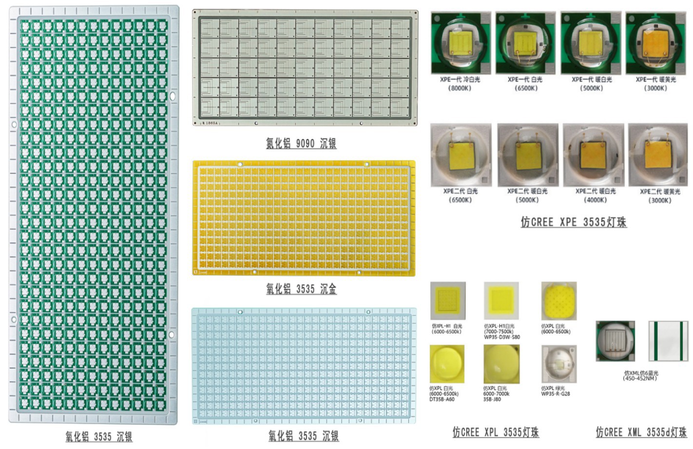
Despite these limitations, DPC excels in realizing fine-line wiring and vertical electrical interconnection, making it particularly suitable for low-current, high-precision device packaging. It is widely used in the fields of laser diodes, optical transceivers, fiber optic communication modules, and other optoelectronic devices where high precision and low thermal damage are required.
2. Thick Film Metallization (TFC): Cost-Effective Mass Production for General-Purpose Applications
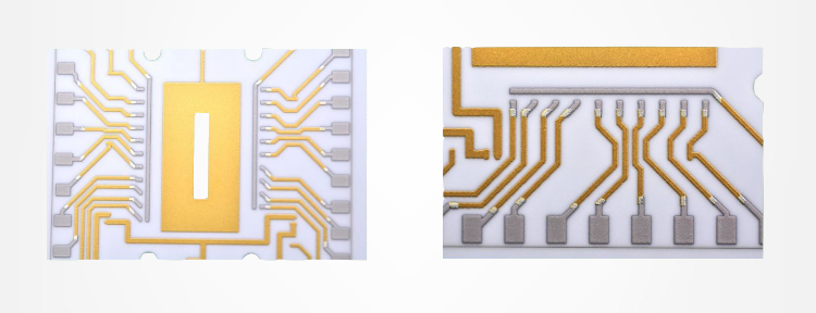
TFC is a mature and low-cost metallization technology that adopts screen printing and high-temperature sintering to form conductive metal layers on ceramic substrates. The core of this process is the metal paste, which is a homogeneous mixture of metal powder, organic binder, and glass frit/metal oxide. The metal powder is the conductive phase, with optional materials including silver (Ag), silver-palladium (Ag-Pd) alloy, gold (Au), gold-platinum (Au-Pt) alloy, copper (Cu), nickel (Ni), and aluminum (Al). Among them, silver and copper are the most widely used in industrial production due to their low resistivity, excellent electromigration resistance, and cost-effectiveness—silver conductive paste alone accounts for more than 80% of the global thick-film metal paste market.
The TFC process flow is relatively simple: first, the metal paste is evenly coated on the ceramic substrate surface through screen printing according to the pre-designed wiring pattern; then, the substrate is dried at a low temperature (100-200°C) to remove the solvent in the paste and improve the adhesion of the wet film; finally, it is sintered at a high temperature (600-900°C) in a controlled atmosphere. During sintering, the organic binder is completely burned off, and the glass frit/metal oxide melts and reacts with the ceramic surface to form a transition layer, which firmly bonds the metal powder particles together and adheres the metal layer to the ceramic substrate.
The main advantages of TFC are low manufacturing cost, simple operation, low requirements for equipment and production environment, and high production efficiency, which is very suitable for mass production of general-purpose ceramic substrates. The sintered thickness of the metal wiring layer is usually between 10 and 20 micrometers, which can meet the basic conductive needs of most low-power electronic devices. However, TFC also has inherent limitations: the precision of screen printing is limited (the minimum line width is usually above 50 micrometers), which makes it difficult to realize ultra-fine wiring; the uniformity of the metal paste and the stability of the sintering process have a great impact on the performance of the metal layer, and it is easy to produce defects such as uneven thickness and poor adhesion; in addition, most commercially available glass frits contain lead, which poses potential hazards to the environment and human health and does not meet the requirements of green production.
3. Direct Bonded Copper (DBC): High-Thermal-Conductivity Solution for Power Electronic Packaging
DBC is a high-performance metallization technology specifically designed for aluminum oxide (Al₂O₃) and aluminum nitride (AlN) ceramics, which are widely used in power electronic packaging. Originating in the 1970s, DBC has been continuously optimized and is now a core technology in the field of power semiconductor modules.
The core principle of DBC is to achieve metallurgical bonding between copper and ceramic through a high-temperature eutectic reaction. Specifically, a certain amount of oxygen is introduced to the surface of the copper plate and the ceramic substrate first; then, the assembly is heated to a temperature range of 1000-1100°C in a controlled atmosphere. At this temperature, copper and oxygen react to form a Cu₂O-Cu eutectic liquid phase (melting point around 1065°C), which has excellent wettability on the ceramic surface. The eutectic liquid phase spreads evenly on the ceramic surface and reacts with the ceramic to form a stable interface transition layer, thereby realizing firm metallurgical bonding between copper and ceramic after cooling.
The key process parameters of DBC include the oxidation time and temperature of the copper plate, oxygen partial pressure during sintering, and cooling rate. These parameters directly affect the formation of the eutectic phase, the quality of the interface transition layer, and ultimately the bonding strength and thermal conductivity of the substrate. DBC ceramic substrates have the advantages of high thermal conductivity, low contact resistance, good mechanical strength, and excellent electrical insulation performance, making them widely used in power semiconductor modules, solar panel components, Insulated Gate Bipolar Transistors (IGBTs), and other high-power electronic devices that require efficient heat dissipation and reliable electrical connection.
However, DBC also has certain technical limitations: the high-temperature eutectic reaction has extremely high requirements on the precision of equipment and process control, and slight deviations in parameters may lead to bonding failure; the bonding strength of DBC is still insufficient for some extreme application scenarios (such as high-vibration, high-impact environments); in addition, the high processing temperature may cause thermal stress and warpage of the ceramic substrate, affecting the dimensional accuracy of the product.
4. Direct Bonded Aluminum (DBA): Improved Fatigue Resistance for High-Temperature Power Applications
Derived from the DBC process, DBA is a modified metallization technology that replaces copper with aluminum as the metal layer. It overcomes some inherent defects of DBC by utilizing the excellent wettability of liquid aluminum on ceramic surfaces and the good thermal fatigue resistance of aluminum.
The working principle of DBA is simpler than that of DBC: when the temperature rises above the melting point of aluminum (about 660°C), the solid aluminum sheet placed on the ceramic surface melts into a liquid state. Liquid aluminum has good wettability on the surface of most ceramics (such as Al₂O₃, AlN) and can quickly spread and adhere to the ceramic surface. With the decrease of temperature, liquid aluminum crystallizes and grows on the crystal nuclei provided by the ceramic surface, forming a dense aluminum layer and realizing firm bonding with the ceramic substrate at room temperature. Unlike DBC, DBA does not require the formation of a eutectic phase through oxidation reaction, but relies on the physical and chemical interaction between liquid aluminum and ceramic to achieve bonding.
DBA ceramic substrates (especially Al₂O₃-DBA and AlN-DBA) have significant performance advantages: they exhibit excellent thermal conductivity, which is comparable to DBC substrates; more importantly, aluminum has a lower coefficient of thermal expansion (CTE) than copper, which reduces the thermal mismatch between the metal layer and the ceramic substrate, thereby significantly improving the thermal fatigue resistance of the substrate. In thermal cycle tests, DBA substrates show fewer interface cracks and longer service life than traditional DBC substrates, making them more suitable for high-temperature, cyclic thermal stress application scenarios.
Nevertheless, DBA also has some drawbacks that restrict its application: first, the process has extremely strict requirements on oxygen content—even a small amount of oxygen in the environment may cause oxidation of liquid aluminum, affecting the bonding quality; second, DBA requires high-precision temperature control and vacuum equipment, resulting in relatively high production costs; third, the aluminum layer thickness in DBA is usually more than 100 micrometers, which makes it difficult to realize fine-line wiring and is not suitable for miniaturized, high-density electronic packaging.
5. Active Metal Brazing (AMB): High-Stability Metallization for Advanced Power Modules
As an upgraded version of DBA, AMB (Active Metal Brazing) further improves the structural stability, bonding strength, and material adaptability of ceramic substrate metallization. It is currently the most advanced and widely used metallization technology in the field of high-power, high-reliability electronic packaging (such as new energy vehicle power modules, high-voltage IGBT modules).
The core principle of AMB is to introduce active elements into the brazing filler metal to realize chemical bonding between the brazing filler metal and the ceramic substrate. The specific process flow is as follows: first, use screen printing to evenly coat the active brazing paste on the surface of the ceramic substrate; then, cover a copper plate (or other metal sheets) on the brazing paste; finally, place the assembly in a vacuum brazing furnace and heat it to a certain temperature (usually 800-950°C) for sintering. During the sintering process, the active elements in the brazing filler metal (such as titanium Ti, zirconium Zr) react with the oxide on the ceramic surface to form a stable intermetallic compound or oxide transition layer, thereby realizing firm metallurgical bonding between the copper plate, brazing filler metal, and ceramic substrate.
The active elements in the brazing paste are usually selected from transition metals in the periodic table, which have strong chemical activity and high affinity for oxides and silicates. Among the various active brazing fillers, Ag-Cu-Ti brazing filler metal is the most mature and widely used after years of research. It has excellent wettability on almost all types of ceramics (including Al₂O₃, AlN, Si₃N₄), high bonding strength, good electrical and thermal conductivity, and stable performance under high temperature and high pressure. Other common active brazing fillers include Cu-Zn-Ti, Ti-Zr-Cu, Sn-Ag-Ti, and Ni-Pd-Ti, which are selected according to specific application requirements and ceramic material types.
Compared with DBC and DBA, AMB has obvious comprehensive advantages: first, it has higher structural stability and bonding strength, and can withstand harsh working environments such as high temperature, high pressure, and strong vibration; second, the entire process can be completed in a single heating cycle, which shortens the production cycle and improves production efficiency; third, it has strong adaptability to ceramic materials and can be used for metallization of various high-performance ceramics; fourth, the copper layer thickness can be flexibly adjusted, and fine-line wiring can be realized by subsequent etching processes, which is suitable for miniaturized and high-density power module packaging. Therefore, AMB technology has become the preferred metallization solution for new energy vehicles, aerospace, smart grid, and other high-end power electronic fields.
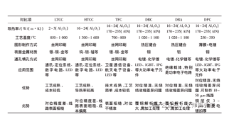
Comparative Overview of the 5 Metallization Processes
| Metallization Process (Abbreviation) | Core Principle | Key Operating Temperature | Typical Metal Layer Thickness | Advantages | Disadvantages | Typical Application Scenarios |
|---|---|---|---|---|---|---|
| Direct Plated Copper (DPC) | PVD sputtering seed layer + electroplating to deposit copper layer | ≤ 300°C | Thin (limited by process), usually several to tens of μm | Low temp (no thermal damage to ceramics), fine-line wiring, vertical interconnection | Plating solution pollutes environment; weak metal-ceramic bonding strength | Laser diodes, optical transceivers, fiber optic communication modules |
| Thick Film Metallization (TFC) | Screen printing metal paste + high-temp sintering (organic binder burned off, glass frit forms transition layer) | 600-900°C (sintering); 100-200°C (drying) | 10-20 μm | Low cost, simple operation, high production efficiency, suitable for mass production | Limited printing precision (min line width ≥50μm); lead-containing glass frit; poor adhesion stability | General-purpose low-power electronic devices, basic conductive packaging |
| Direct Bonded Copper (DBC) | High-temp eutectic reaction (Cu-O forms Cu₂O-Cu eutectic phase) to achieve metallurgical bonding | 1000-1100°C | Flexible, usually tens to hundreds of μm | High thermal conductivity, low contact resistance, good mechanical strength | High equipment/process precision requirements; insufficient bonding strength for extreme scenarios; thermal warpage risk | Power semiconductor modules, solar panel components, IGBTs |
| Direct Bonded Aluminum (DBA) | Liquid aluminum wets ceramic surface, crystallizes and bonds with ceramic during cooling | ≥ 660°C (aluminum melting point) | ≥ 100 μm | Excellent thermal fatigue resistance; low thermal mismatch; good thermal conductivity | Strict oxygen content control; high production cost; not suitable for fine wiring | High-temperature, cyclic thermal stress power electronic devices |
| Active Metal Brazing (AMB) | Active elements (Ti/Zr) in brazing paste react with ceramic to form transition layer, achieving metallurgical bonding | 800-950°C | Flexible, tens to hundreds of μm (adjustable) | High structural stability/bonding strength; short production cycle; strong ceramic adaptability; fine wiring available | Higher cost than DBC/DBA; requires vacuum brazing equipment | New energy vehicle power modules, high-voltage IGBT modules, aerospace power electronics Note: The above parameters and application scenarios are typical values in industrial production, and can be adjusted according to specific process optimization and project requirements. |
Note: The above parameters and application scenarios are typical values in industrial production, and can be adjusted according to specific process optimization and project requirements.
trending news
Contact Us