


Sorry, no sales person is available right now to take your call. Pls leave a message and we will reply to you via email as soon as possible.
Material Selection and Manufacturing Pitfalls for High-End PCBs in AI Compute Infrastructure
2026-11-13
Investment in AI compute infrastructure continues to scale, and AI servers and switches are driving growing demand for high-layer-count boards, advanced HDI (High-Density Interconnect) structures, and high-speed laminates. In procurement and engineering delivery, however, recurring issues often determine yield and lead time: extended lead times for high-speed materials, batch-to-batch Dk/Df variation that compromises signal integrity (SI), and uncontrolled expansion and shrinkage in high-layer-count lamination that leads to layer misalignment. This article reviews the core technical requirements for AI compute boards and outlines practical practices for avoiding common pitfalls, based on frontline PCB manufacturing and quality-control experience.
1. Core Parameters: The Foundation of Performance
AI servers handle high data throughput. The adoption of PCIe 5.0/6.0 and 112G/224G high-speed serial links places stringent requirements on the high-frequency characteristics of PCB base materials.
Dielectric Constant (Dk) and Dissipation Factor (Df)
At test frequencies of 10 GHz and above, AI server boards commonly use Ultra Low Loss or Extreme Low Loss grade laminates. Df is typically controlled below 0.003 to help reduce energy attenuation of high-frequency signals during transmission. Dk should also remain stable, with a typical tolerance of ±0.05, to support consistent phase performance.
Glass Transition Temperature (Tg) and Thermal Resistance
The rising power consumption of compute chips increases the thermal load on boards. Laminate Tg — the critical temperature at which the material transitions from a glassy to a rubbery state — is commonly required to be ≥170°C, and in some applications above 180°C. T260/T288 metrics (delamination time at 260°C/288°C) should also be reviewed to help reduce the risk of popcorning or delamination under repeated high-temperature lead-free reflow cycles.
Impedance Control Accuracy
High-speed signal traces require tight control of characteristic impedance. Typical targets are 50 Ω ±10% for single-ended impedance and 100 Ω ±10% for differential impedance. For higher-speed interfaces, the tolerance band may be tightened to ±8% or narrower, depending on the interface and stack-up.
2. Manufacturing Challenges and Process Control
AI server PCBs commonly range from 20 to over 30 layers, often combined with any-layer HDI structures, which increases manufacturing complexity.
High-Layer-Count Lamination and Dimensional Stability
As layer count increases, resin flow and dimensional expansion/shrinkage of inner-layer cores during lamination become more difficult to control. Engineering practice calls for a symmetrical stack-up design with pre-calculated expansion and shrinkage compensation. During lamination, the ramp-up rate, dwell time, and pressure curve should be matched carefully to help prevent core shifting, measling, or interlayer registration deviation.
Backdrill Control
To reduce reflections caused by signal stubs at via ends, backdrilling is widely used on high-layer-count boards. Controlling backdrill depth and residual stub length is a core challenge; stub length is commonly targeted at ≤10 mil. This requires high Z-axis accuracy from the drill machine, together with accurate board-thickness and copper-thickness measurements used for depth compensation.
Surface Finish and Roughness Control
To help reduce skin-effect loss on conductor surfaces, copper foil surface roughness (Rz) on high-speed signal traces should be tightly controlled. HVLP (Very Low Profile) copper foil is commonly selected. Surface finishes are often ENIG (Electroless Nickel Immersion Gold) or hard gold plating; gold thickness should be uniform to help avoid nickel corrosion that could degrade high-frequency signal performance.

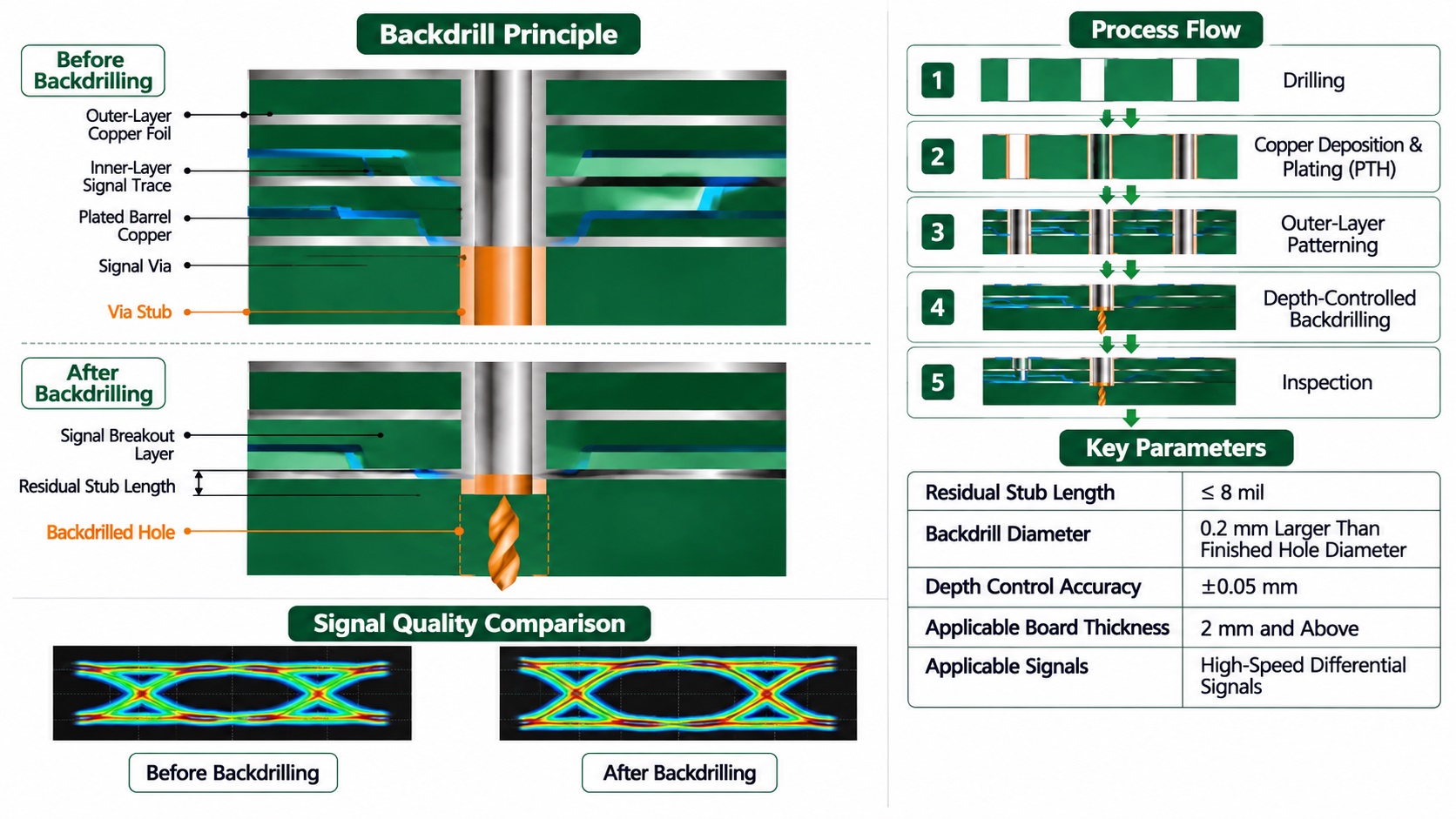
Schematic of the backdrilling process on a high-speed PCB
3. Practical Checklist and Pitfall Avoidance for Engineers
Based on project delivery experience, the table below summarizes common issues, associated risks, and recommended mitigation practices.
| Common Pain Point | Potential Risk | Avoidance and Practical Recommendations |
| Poor batch-to-batch laminate consistency | Dk/Df variation across batches can cause impedance out-of-spec in TDR (Time Domain Reflectometry) testing and invalidate SI simulation. | Require suppliers to provide same-batch COC/COA reports during procurement; perform cross-section and impedance coupon testing on first articles to verify measured Dk. |
| Inadequate MSL moisture-control management | After absorbing moisture, higher-grade laminates may develop internal microcracks or popcorning during reflow as trapped moisture expands. | Follow IPC/JEDEC J-STD-033 for MSL (Moisture Sensitivity Level) control. If boards remain unmounted beyond the allowed exposure time after bag opening, bake them to remove moisture per specification. |
| Perfunctory DFM review | Layout trace width/spacing approaching the factory's process limits can result in excessive etch-back and low impedance. | Involve the PCB manufacturer's DFM (Design for Manufacturability) review early in the layout stage. Confirm the factory's process capabilities (e.g., minimum trace width 3 mil, minimum hole diameter 0.1 mm) and leave a reasonable tolerance band. |
| Copper thickness and impedance mismatch | Inner-layer copper thickness tolerances that are not accounted for can lead to errors in dielectric thickness calculation and, ultimately, impedance deviation. | Confirm target copper thickness with the board manufacturer during design (e.g., 1 oz finished copper), and enter the actual etched trapezoidal cross-section parameters into the impedance simulation tool for fine-tuning. |
4. Conclusion
The AI compute wave brings growth opportunities to the PCB industry, yet delivering high-end compute boards is not simply a matter of adding capacity. It is a combined test of materials science, precision manufacturing, and quality control.
For hardware engineers and procurement professionals, the macro industry narrative should be grounded in the practical realities of manufacturing. During selection and design, the physical limits of high-speed materials and the actual process capabilities of the factory should be considered; during production, a data-based quality traceability system should be established. Embedding the DFM mindset throughout the process supports reliable, high-yield delivery of compute platforms.
trending news
Contact Us