



Sorry, no sales person is available right now to take your call. Pls leave a message and we will reply to you via email as soon as possible.
How Stacked Vias Improve Density and Performance in HDI PCBs
2026-11-11
Key Takeaways
· Stacked vias align microvias vertically in a single column, often combined with via-in-pad placement, to shrink breakout area, shorten interconnect paths, lower parasitic inductance, and improve vertical heat transfer compared with staggered arrangements.
· They can help reduce total layer count and support fine-pitch BGA fanout, but they require sequential lamination, reliable via filling, tight registration, and clearly defined design rules.
· The choice between stacked and staggered vias is a trade-off among routing density, electrical and thermal performance, manufacturing tolerance, and cost.
The Layout Problem Stacked Vias Solve
As package pitches tighten and boards carry more layers, conventional through-hole escape runs into three limits at once: pads and clearance rings consume surface area, escape traces detour around the package, and long via stubs complicate high-speed transitions. Stacked vias address these by connecting adjacent layers through one straight column rather than a stepped chain.
This guide covers how the structure works, where it helps most, the constraints that keep it reliable, and the process controls behind a stable yield.
What Stacked Vias Are
A stacked via places two or more vias on the same vertical axis, one above another, so adjacent-layer connections form one continuous column. In a typical HDI buildup, a microvia spanning L1–L2 sits directly over a microvia spanning L2–L3, which may continue into a buried via for deeper layers.

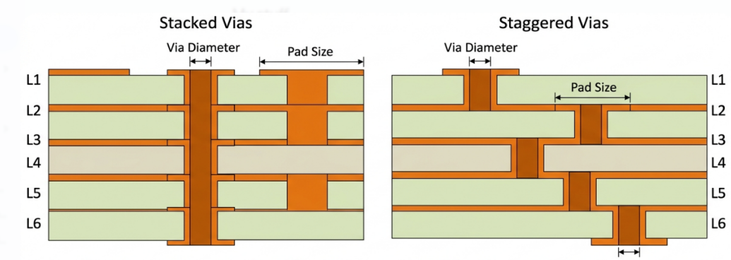
By contrast, staggered vias are offset horizontally between neighboring layers; adjacent vias meet on a shared intermediate pad instead of sharing an axis. A useful analogy: stacked vias form a straight elevator shaft, while staggered vias follow a staircase.
| Aspect | Stacked vias | Staggered vias |
| Alignment | Same vertical axis | Horizontally offset layer to layer |
| Routing density | High; compact pad footprint | Lower; offset pads take more space |
| Signal path | Direct and shorter | Longer through lateral offsets |
| Process tolerance | Tight alignment required | More forgiving |
| Cost | Higher; sequential lamination and fill | Lower; standard HDI flow |
| Heat transfer | Strong vertical heat column | Adequate, less direct |
Staggered vias remain a practical choice where tolerance and cost matter more than maximum density. Stacked vias are preferred when the priority is dense fanout, low parasitic inductance, or a direct thermal path.
Why Stacked Vias Matter in Fine-Pitch HDI
Fine-pitch BGAs leave little room between pads for escape traces routed to off-pad vias. Stacked vias make via-in-pad practical: the via lands inside the package pad, is filled with conductive or non-conductive material, and capped with copper. Removing the pad-to-via escape trace reclaims routing area around the package; how much area is recovered depends on ball pitch, pad geometry, and fanout strategy rather than a fixed percentage.
Key Benefits
Higher routing density, fewer layers
Because the via runs straight and often sits in-pad, area otherwise taken by via pads, clearance rings, and escape traces is returned to the routing channel. In compact modules and dense processor boards, this can relieve pressure on signal layers; layers that would otherwise carry escape routing may instead support power and ground distribution. Fewer layers, where achievable, tend to carry through to thinner profiles, shorter lamination and drill-plate sequences, and lower material and weight overhead — though the actual layer count is set by the full netlist, not the via style alone.
Cleaner high-speed transitions
A straight vertical transition shortens stub length and removes the lateral segments a staggered chain requires. Above roughly 1 GHz, via-transition parasitics matter; a well-formed stacked via with considered antipad geometry typically shows lower loop inductance than a staggered equivalent (order of a few tenths of a nanohenry; exact values depend on stackup and pad design). The practical gains are shorter stubs than through-hole connections, a smaller loop area, easier placement of nearby return vias, and a useful column for thermal escape.
Design Constraints, Organized by Stage
Before locking the layout
· Aspect ratio: via depth over diameter sets what drilling and plating can support. Mechanically drilled vias commonly run near 10:1 (advanced processes higher); laser HDI microvias stay near or below 1:1, with diameters in the fine-microvia range. Confirm current limits with the fabricator.
· Column height: most shops keep a column to a few microvias; beyond that, registration error and thermal stress accumulate faster than they can be controlled.
· Capture pad sizing: pad and target dimensions should leave room for layer-to-layer misalignment rather than being sized to nominal registration alone.
During the buildup
· Fill before the next via: each microvia is filled and planarized before another is drilled on top; an unfilled cavity can open cracks under thermal cycling.
· Fill material choice: copper fill favors electrical and thermal performance; non-conductive epoxy is a lower-cost option adequate for signal vias.
· Planarization quality: a level surface is what the next via lands on; uneven fill or residual recess undermines the next registration.
Before release to production
· Reference the HDI design standard: IPC-2226 defines microvia and stacked-via configurations and classifies HDI buildups by via structure.
· Confirm capability early: aspect-ratio limits, minimum diameter, maximum column height, and fill options vary by supplier; verify them against the actual stackup before layout is finalized.
Stackup and Thermal Integration
Stacked vias are part of the overall layer stackup, not a standalone feature. Dielectric thicknesses set microvia depth and therefore aspect ratio. Common HDI buildups are written 1+N+1 or 2+N+2: the leading and trailing numbers are sequential buildup layers on each side, and N is the core layer count. A 2+4+2 stack, for example, has two buildup layers on each side of a four-layer core — eight layers total — and supports two levels of stacked microvias.
| Stackup | Total layers | Microvia stack levels | Typical use |
| 1+N+1 | 4–8 | 1 (single microvia) | Mobile devices, IoT modules |
| 2+N+2 | 6–12 | 2 (two stacked microvias) | Smartphones, networking gear |
| 3+N+3 | 10–16 | 3 (three stacked microvias) | High-end processors, FPGA boards |
| Any-layer HDI | 8–20+ | All layers interconnected | Advanced SiP, military/aerospace |
Stacked vias are also effective as thermal via arrays under power components. A column of stacked vias running from the top thermal pad to a ground plane or heatsink layer creates a direct heat path. With adequate via density and fill quality, a copper-filled stacked via array can reach roughly 100–200 W/mK, far above the ~0.3 W/mK of surrounding FR-4.
Manufacturing Challenges
Registration and plating
The main manufacturing challenge is layer-to-layer registration. Each upper via must land on the filled, planarized pad of the via below. Poor alignment can leave a partial pad landing — a weak joint that may fail during thermal cycling. Typical HDI registration tolerance is about ±25–50 µm per layer, and these tolerances accumulate across a three-via stack. High-end production uses optical alignment, layer fiducials, and X-ray inspection to keep alignment within limits.
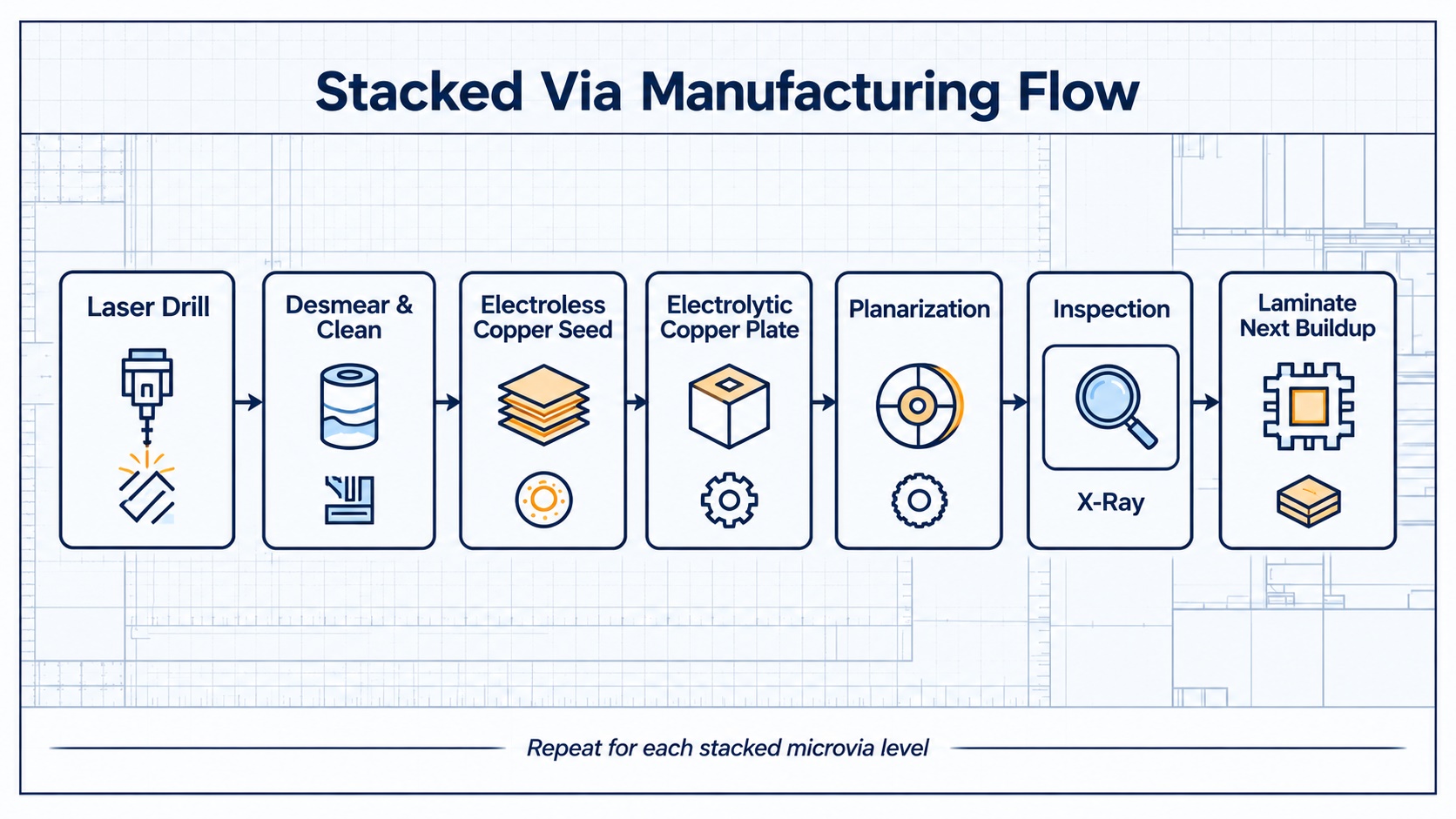
A typical sequential fill and plating flow:
1. Laser-drill microvias (UV or CO₂)
2. Desmear and clean holes
3. Deposit electroless copper seed
4. Electroplate copper to fill vias
5. Planarize surface (mechanical or chemical-mechanical)
6. Inspect and verify fill quality
7. Laminate the next buildup layer and repeat

KINJI GROUP: Stacked-Via HDI Manufacturing Support
HDI capability for complex via stacks
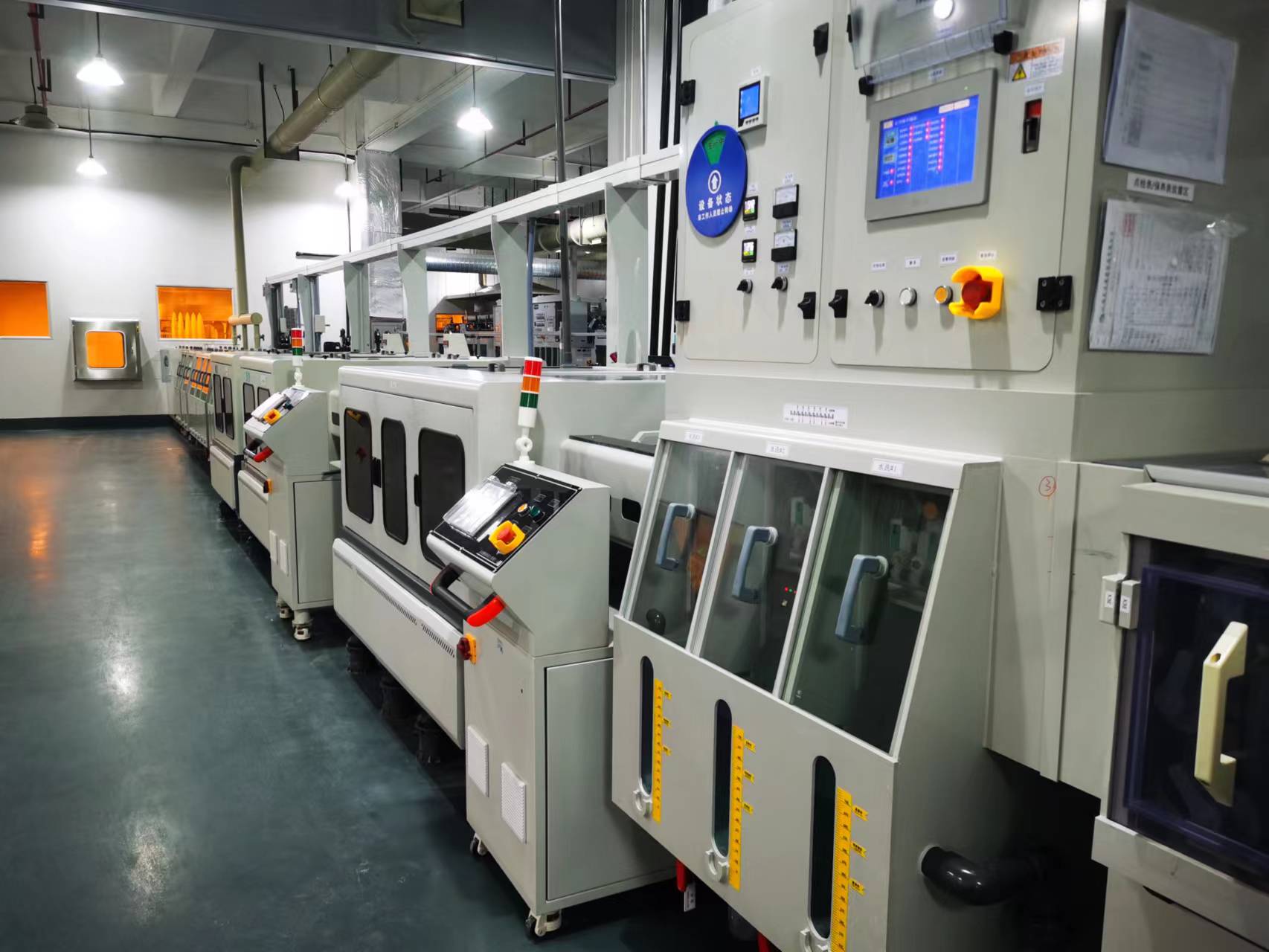
KINJI GROUP supplies HDI PCB fabrication covering 1+N+1, 2+N+2, and higher-order buildups, with the alignment control and fill quality required for stacked microvias. Production lines use laser drilling for fine-diameter microvias and support both copper and non-conductive epoxy via fill, with planarization controlled to the tolerances needed for reliable stacking. Capabilities span compact two-level stacks for IoT modules through multi-level stacks for processor and FPGA boards; exact via diameter, stack height, and fill options are confirmed per project through DFM review.

DFM review and yield-oriented production
The DFM review is a key step before production. After the Gerber files are submitted, engineering checks via settings, aspect ratios, pad dimensions, and stackup compatibility against the process capability. Potential issues — microvias outside the recommended aspect ratio, capture pads too small for reliable registration, or fill requirements left unspecified — are flagged early, avoiding costly changes after tooling.
FAQ
What is a stacked via?
Two or more vias placed directly above one another on the same vertical axis. Each via connects adjacent layers; together they form a continuous vertical interconnect across multiple layers. Each via must be filled and planarized before the next one is drilled.
What is the difference between stacked and staggered vias?
Stacked vias share one vertical axis; staggered vias are offset horizontally between layers. Stacked vias give higher density and shorter paths but require more complex processing. Staggered vias are easier and cheaper to manufacture but consume more routing space.
How many microvias can be stacked?
Most suppliers reliably support two to four microvias per column. Beyond four, cumulative registration error and thermal stress rise sharply. Confirm the maximum stack height with your fabricator.
Are stacked vias more expensive than standard vias?
Usually yes: each level adds sequential lamination, laser drilling, filling, and planarization steps. However, if stacked vias allow you to reduce total layer count, the overall board cost can be comparable or lower.
Conclusion
Stacked vias are a core enabler of dense, high-performance HDI designs. Via-in-pad placement, shorter interconnects, reduced layer count, and direct thermal paths help engineers work around the limits of conventional vias as products shrink and speed requirements rise. They do require disciplined design rules and mature manufacturing, but the gains in routing density, signal integrity, and thermal performance generally justify that complexity. KINJI GROUP supports stacked-via HDI projects through DFM review, controlled fill and alignment, and inspection-oriented quality processes, helping designs move from layout to production with a stable yield.
trending news
Contact Us