



Sorry, no sales person is available right now to take your call. Pls leave a message and we will reply to you via email as soon as possible.
Concentric Rings for Uniform Fields, Heavy Copper for High Current | KINJI 7oz Ultra-Large Circular Heavy-Copper Specialty PCB
2026-11-09
Thermal uniformity, field consistency, and long-term stability are the metrics that determine yield and precision in semiconductor vacuum chambers, optical coating systems, precision heat-treatment furnaces, and RF/mmWave test rigs. As equipment grows in size, the limitations of conventional rectangular PCBs become more pronounced in warpage, heat distribution, field balance, and current-carrying capacity — failure points that must be carefully controlled in demanding applications.
With 29 years focused on high-precision specialty PCBs, KINJI developed the ultra-large circular concentric-ring specialty PCB to address these challenges. Built on a concentric-ring topology, combined with production-grade heavy-copper processes and vacuum-grade ultra-clean surface finishing, the board delivers an integrated carrier-board solution for uneven thermal and magnetic field distribution on large panels. It serves four high-end sectors: semiconductor, PV & display, precision heat treatment, and RF testing.
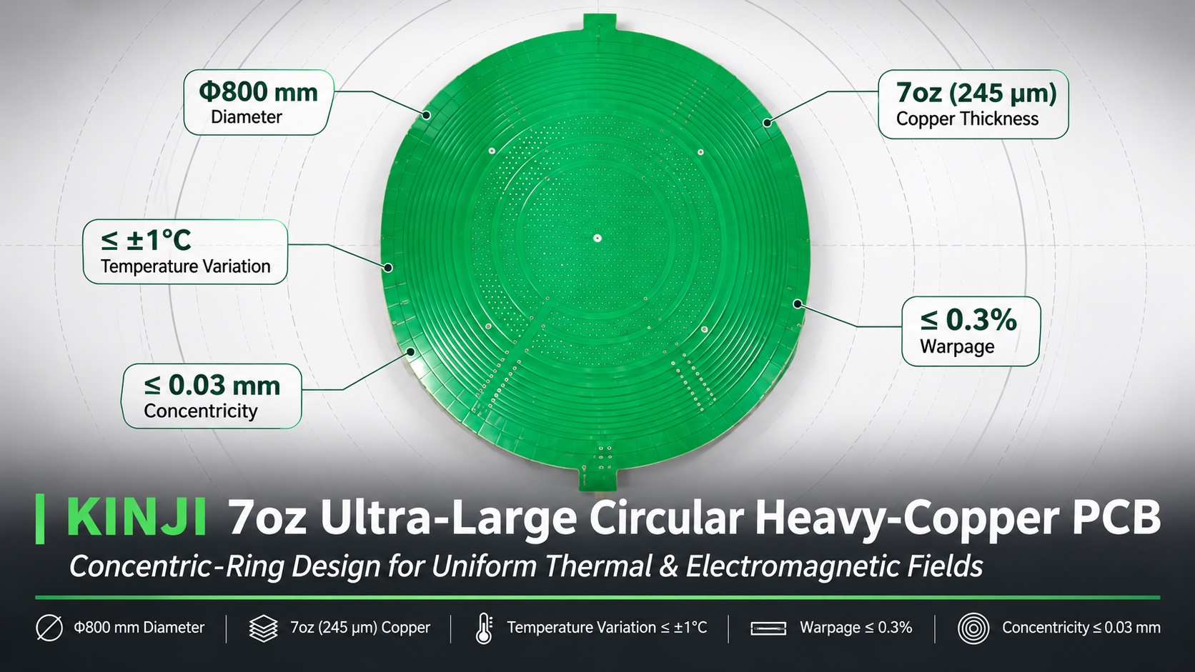
Core Strength: Concentric Topology Redefining Uniformity for Large Panels
The board uses a symmetrical, precision-controlled construction, with a maximum finished diameter of 800 mm and a standard finished thickness of 1.1 mm. It is built on selected high-Tg 180 FR-4 material rated for continuous operation at 220°C, suited to high-vacuum, high-temperature, continuous-duty environments.
The concentric-ring independent-circuit zoning design divides the full heating and radiation area into modular zones, with precise, independent power control per ring band. This delivers balanced control across the thermal field, electromagnetic field, and radiation field, establishing a quantifiable process baseline for large-panel uniformity.
Precision conductive gold fingers, a central datum locating hole, and four high-precision mounting holes provide stable, durable electrical connections while supporting micron-level alignment and integrated assembly.
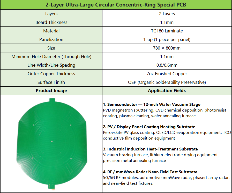
Application Scenarios, Matched to Precision Manufacturing
12-Inch Wafer Vacuum Stage (Semiconductor)
Equipment compatibility: PVD magnetron sputtering, CVD deposition, photoresist coating, plasma cleaning, wafer annealing furnaces, and other core process equipment.
Value: The concentric-zone temperature control holds panel temperature variation to ≤±1°C, supporting uniform wafer coating, deposition, and annealing and helping improve process yield. The dedicated vacuum-grade clean OSP finish is designed for low metal outgassing and low particle release to reduce chamber contamination. It supports 160°C continuous operation and 200°C short-term peak temperatures, matching demanding semiconductor process requirements.
PV / Display Panel Coating Heating Substrate
Equipment compatibility: Perovskite PV glass coating, OLED/LCD vacuum evaporation, TCO conductive film deposition, and other optical coating equipment.
Value: Uniform heating across the ultra-large panel improves uneven film thickness and transmission variation on large optical substrates, enhancing coating quality on PV glass and display panels. The 7oz thick copper layer carries high current, delivers fast thermal response and precise temperature hold, and helps reduce coating defects such as uneven film, delamination, and color variation.
Industrial Precision Induction Heat-Treatment Substrate
Equipment compatibility: Vacuum brazing furnaces, lithium-electrode drying, precision metal annealing furnaces, and other high-end heat-treatment equipment.
Value: Precision concentric-ring coils build a uniform electromagnetic induction field across the working area, ensuring synchronized, even heating of workpieces. This addresses uneven local temperature, deformation, cracking, and performance dispersion associated with conventional heat treatment, supporting consistent quality across production batches.
RF / mmWave Radar Near-Field Test Substrate
Equipment compatibility: 5G/6G RF modules, automotive mmWave radar, phased-array radar, and high-end near-field test fixtures.
Value: Regular concentric-ring traces create a highly uniform, consistent electromagnetic radiation field, providing a stable, traceable, repeatable test reference for 5G/6G RF modules, automotive radar, and phased-array radar. It reduces test error caused by uneven radiation on conventional carriers, improving RF measurement accuracy and fixture calibration reliability.
Process Control: Quality Built to Strict Standards
KINJI operates two manufacturing bases in Shenzhen and Jiangxi, with 16,000 ㎡ of standardized cleanroom space, a monthly capacity of 100,000 ㎡, and a 200-person engineering and R&D team, backed by 29 years of specialty PCB experience. The full process runs 36 controlled steps under closed-loop management, with UL, ISO 9001, ISO 13485, and IATF 16949 certifications, delivering stable, reliable core carriers for high-end equipment.
1. Large-Panel Deformation Control for Flatness
To address stress-induced deformation on large panels, all base material undergoes a 48-hour constant-temperature resting period for stress relief, paired with batch-specific CTE compensation to control dimensional deviation from the outset. Only Grade-A, high-stability, high-heat-resistance original materials are used. Lamination uses segmented intelligent temperature control with a ramp rate held to ≤2°C/min, combined with symmetrical stacking to reduce directional stress. Finished panels are fully inspected on a precision granite platform, with board warpage ≤0.3%, meeting the assembly and sealing requirements of high-end equipment.
2. Micron-Level Trace Formation for Concentric Accuracy
Large-format parallel-light precision exposure delivers ring-trace width uniformity within ≤±0.05 mm, ensuring consistent trace specifications across all ring bands. The etching line uses a zoned intelligent spray-pressure system to control outer-ring over-etching and inner-ring copper residue. Layer-to-layer registration is ≤0.04 mm, with full-board AOI optical inspection to trace defects. Locating and datum holes are formed in one precision operation; overall concentricity is ≤0.03 mm, keeping all ring bands coaxial for balanced thermal and magnetic output.
3. Vacuum-Grade Clean Process for Cleanroom Conditions
A high-temperature-resistant precision matte solder mask is applied to a controlled thickness of 20–35 μm, with low pinhole and bubble levels and controlled outgassing and particle release in high-temperature vacuum environments, suited to ultra-clean semiconductor and optical coating processes. The OSP anti-tarnish film is 0.2–0.5 μm thick, applied after multi-stage rinsing with 18 MΩ ultrapure water to control ionic residue and metal release and reduce contamination of precision components and vacuum chambers. Contact pads carry a gold finish ≥0.05 μm, providing wear resistance and oxidation resistance for frequent mating cycles and long-term stable operation.
4. Full Electrical Testing for Long-Term Reliability
Quality control covers 100% board inspection and per-board traceability: 100% continuity testing to catch micro-open and hidden-open faults; a 2 kV AC layer-to-layer dielectric withstand test held for 5 minutes, with no breakdown or flashover. Full-current temperature rise is measured and controlled: temperature variation ≤1°C on semiconductor-grade boards and ≤3°C on general-purpose versions. Boards survive 100 thermal cycles from -40°C to 180°C with no delamination, cracking, or performance degradation, supporting long-term operation in demanding conditions.
5. Cleanroom Manufacturing and Vacuum Packaging for Delivery Quality
Core processes — etching, solder mask, OSP, and precision cleaning — run in a Class 10,000 cleanroom to control particulate contamination at the source. Finished boards are packed individually in vacuum anti-static packaging with protective structure and a desiccant system to prevent transit damage, oxidation, and moisture, delivering boards ready for use on arrival.
Delivery and Service
Ultra-large panel production capacity: For difficult specialty categories such as Φ800 mm circular PCBs, KINJI covers the full flow from prototyping and pilot validation to volume delivery, with mature designs and controlled lead times to address the common challenges of fabrication, volume ramp-up, and delivery for ultra-large specialty boards.
Established heavy-copper process: The 7oz (245 μm) ultra-heavy copper process is standardized and produced at scale, providing a mature solution to high-temperature burn-out, insufficient current capacity, and uncontrolled temperature rise on conventional thin-copper boards, supporting equipment stability under high-current, high-temperature continuous duty.
Vacuum-environment customization: The proprietary vacuum-grade clean OSP preparation process replaces high-outgassing finishes such as ENIG and HASL where applicable, with low metal outgassing and low particle release for ultra-clean vacuum environments in semiconductor and optical coating equipment, delivered as a customized solution.
Key precision metrics: Concentricity ≤0.03 mm, trace-width uniformity ±0.05 mm, and warpage ≤0.3% provide the physical accuracy base for uniform temperature, uniform field, and high-precision operation in high-end equipment.
End-to-end closed-loop service: KINJI offers a full range of specialty materials and customized precision process solutions, covering design iteration, structural optimization, sample validation, reliability testing, and volume delivery. Business covers 100+ countries and regions, serving 100,000+ high-end manufacturing customers, with extensive experience supporting global high-end projects.
To evaluate specifications for your custom requirements, please reach out to the KINJI engineering team for tailored solutions and sample evaluation support.
trending news
Contact Us