


Sorry, no sales person is available right now to take your call. Pls leave a message and we will reply to you via email as soon as possible.
High-Frequency High-Speed PCBs: The Core Carrier for Computing and Communication Hardware — Kinji Group's Full-Chain Solutions
2026-10-28
Driven by frontier industries such as 6G research, AI computing clusters, automotive millimeter-wave radar, and satellite communications, signal frequencies exceeding 1GHz and transmission rates surpassing 10Gbps have become the industry norm. Conventional FR-4 materials struggle to effectively suppress high-frequency signal attenuation and crosstalk. As the physical foundation of hardware systems, high-frequency high-speed PCBs—spanning material selection, stack-up design, and process control—directly determine the signal integrity (SI) and power integrity (PI) of the entire equipment. Leveraging its advanced PCB manufacturing capabilities, Kinji Group has built a full-process high-frequency high-speed board delivery system covering simulation-based stack-up design, specialty material selection, hybrid lamination processes, and finished-product reliability verification, offering customized PCB solutions across multiple industries.
I. Core Value and Application Scenarios of High-Frequency High-Speed PCBs
High-frequency high-speed PCBs are developed specifically for high-frequency signals above 1GHz and ultra-high-speed data transmission above 10Gbps. By combining low-loss specialty substrates such as Rogers and PTFE with high-precision impedance control processes, they ensure stable signal transmission in complex electromagnetic environments—an indispensable foundation for high-performance computing and communication systems.
6G Communications and Next-Generation Base Stations
Supports low-loss signal transmission in millimeter-wave bands above 24GHz, accommodates the high-density integration requirements of Massive MIMO arrays, and enables ultra-wide bandwidth and ultra-low latency communications. Kinji delivers customized millimeter-wave high-frequency boards using hybrid lamination of Rogers TSM-DS3M and Shengyi S1000-2M, integrating precision high-frequency routing and dedicated thermal structures to meet the stringent electrical requirements of base station RF front-ends.
AI Supercomputing and Computing Clusters
Carries NVLink 5.0 (900GB/s) and PCIe 7.0 ultra-high-speed interconnect links, eliminating data transmission bottlenecks in massively parallel computing. Kinji provides PCBs based on ultra-low-loss high-speed materials such as TUC M8U and Megtron6/7, compatible with 800G/1.6T optical modules and GPU cluster interconnects, minimizing high-speed signal transmission delay.
Intelligent Driving and Automotive ADAS
Compatible with 77GHz/120GHz millimeter-wave radar and LiDAR signal processing, with strong anti-interference capability and stable operation across the -40°C to 85°C automotive-grade wide-temperature range.
Satellite Communications and Aerospace
Products withstand cosmic radiation and extreme temperature fluctuations, providing stable high-frequency signal links for spaceborne phased-array antennas and avionics systems while meeting stringent mechanical strength requirements. A typical example is Kinji's 8-layer satellite communication PCB: utilizing an HJY350A+S1000-M high-frequency hybrid structure, 0.2mm minimum aperture, 1-7/2-8 blind via technology, and hybrid lamination of S1000-2MB and HY350A-M-P high-frequency prepreg, it meets the low-loss requirements of satellite communication RF links.

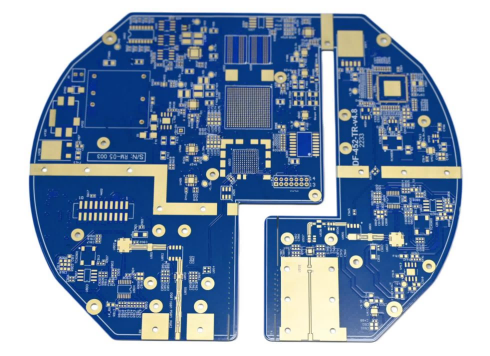
The image shows a precision RF PCB made with Rogers RO4350B high-frequency hydrocarbon material. Its uniform dielectric properties and low loss make it a core foundation for 5G base stations, RF modules, and other high-performance scenarios. We provide full-process precision control from material selection to impedance control.
II. Material Selection System: Matching Performance and Cost, Balancing Loss and Manufacturability
The performance ceiling of high-frequency high-speed PCBs is determined by the substrate. Leveraging a global supply chain and an experienced process team, Kinji provides differentiated material solutions tailored to project dielectric properties, loss targets, and cost objectives. Mainstream material systems fall into five categories:
PTFE (Polytetrafluoroethylene) Series: Dk≈2.1, Df<0.001, offering extremely stable electrical performance and excellent weather resistance for ultra-high-frequency radar, aerospace satellites, and other scenarios with the highest signal integrity requirements.
Rogers RO4350B: Dk=3.48, Df=0.0037, easy to process—the golden balance between performance and cost. Widely used in 5G macro/micro base station antennas and RF front-end modules. Kinji processes Rogers RO4350B hydrocarbon precision RF PCBs, leveraging uniform dielectric properties and low loss to achieve full-process control from material selection to impedance control.
Rogers RO5880 Millimeter-Wave Specialty Material: Ultra-low loss Df=0.0009, low dielectric constant, suitable for millimeter-wave communications, automotive radar, and high-end RF test components.
TUC M8U Ultra-Low-Loss (ULL) Material: Dk=2.9–3.1, Df≤0.0018, designed specifically for AI computing clusters and high-speed interconnects, ensuring extremely low transmission delay for high-speed signals.
High-Speed FR-4 (Megtron6/7): Dk=3.3–3.5, cost-effective, balancing transmission performance and mass-production manufacturability—the mainstream substrate for data center servers and core switches.
For material control, Kinji has established strict incoming inspection standards, combined with vacuum lamination and LDI laser direct imaging processes, ensuring high-frequency board yield and electrical performance consistency.
III. Core Process Control: Four Key Stages Ensuring Hybrid High-Frequency Board Quality
For high-frequency boards—especially heterogeneous material hybrid structures—process design directly affects signal transmission quality and long-term stability. Kinji masters high-frequency hybrid stack-up architecture design and full-process manufacturing, using a sub-card plus main-card stepwise lamination scheme to produce complex multilayer hybrid boards. A typical 8-layer hybrid board process is divided into two stages: sub-card fabrication and main-card lamination:
Sub-cards L1-L2/L7-L8: Cutting → Drilling → Electroless copper & panel plating → Inner-layer circuitry → Inner-layer AOI → Browning → Transfer to main-card lamination;
Sub-cards L3-L4/L5-L6: Cutting → Inner-layer circuitry → Inner-layer AOI → Browning → Transfer to main-card lamination;
Main card L1-L8: Lamination → Debrowning → Copper reduction → Drill in-pad vias → Electroless copper & panel plating → Primary circuitry → Plating → Polishing → Panel tin plating → Back drilling → Outer-layer etching → Resin plugging → Drilling → Electroless copper & panel plating → Outer-layer circuitry → Gold plating → Film stripping → Alkaline etching → Outer-layer AOI → Electrical test → Pre-solder-mask treatment → Solder mask exposure → Legend → Post-cure → Testing → Profiling → Final inspection → Packaging.
Manufacturing focuses on four key control points:
Simulation-based stack-up pre-design: SI/PI simulation predicts and pre-empts potential risks such as impedance discontinuities and signal attenuation, with customized stack-up dielectric parameters;
Precise lamination curve control: Dynamic temperature and pressure regulation ensures uniform dielectric layer thickness across different materials, improves adhesion between dissimilar materials, and eliminates delamination risks in hybrid boards;
Microvia drilling optimization: High-precision drill bits and process parameter tuning reduce hole-wall roughness and resin smear, preventing high-speed signal loss at via transitions;
In-process impedance monitoring: Integrated coupon test strips collect impedance data throughout the process with closed-loop verification, ensuring impedance control accuracy meets specifications.
IV. Kinji High-Frequency High-Speed PCB Production Cases
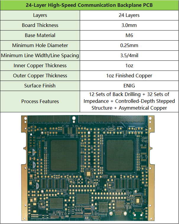
Case 1: 24-Layer High-Speed Backplane
Board thickness 3.0mm, M6 ultra-low-loss high-speed material; line width/spacing 3.5/4mil, minimum aperture 0.25mm, immersion gold surface treatment. Process includes 12 sets of back drilling, full-process impedance control, controlled-depth stepped slots, and positive/negative copper processes, targeting data center high-speed interconnect backplanes and reducing signal loss from stub effects.

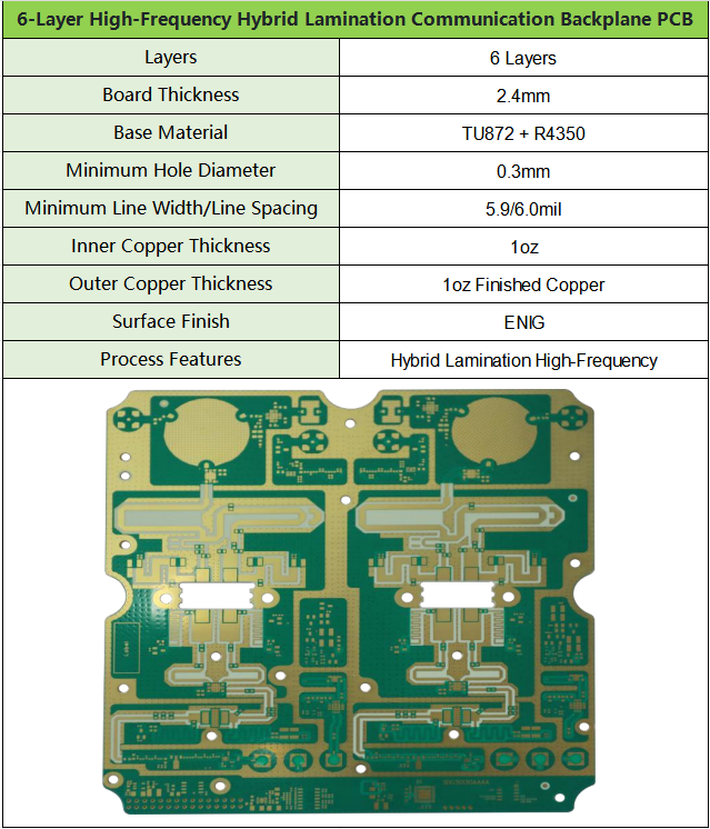
Case 2: 6-Layer Communication High-Frequency Hybrid Board
Board thickness 2.4mm, TU872+Rogers RO4350 hybrid lamination; line width/spacing 5.9/6.0mil, minimum aperture 0.3mm, immersion gold process. Adopts FR4+hydrocarbon high-frequency material hybrid lamination, balancing RF signal transmission performance with manufacturing cost—widely used in communication RF units.

Conclusion
As AI computing, millimeter-wave communications, and the satellite internet industry continue to advance, demand for high-frequency high-speed PCBs will keep growing, raising the bar for multilayer hybrid lamination, impedance control, back drilling, and blind/buried via processes. Kinji Group remains deeply committed to high-frequency high-speed PCB technology, integrating material selection, simulation design, precision manufacturing, and reliability testing across the entire chain—delivering stable and reliable customized high-frequency high-speed PCB solutions for communications, AI computing, automotive, and aerospace customers, empowering high-end hardware products to achieve signal performance breakthroughs.
trending news
Contact Us