

Sorry, no sales person is available right now to take your call. Pls leave a message and we will reply to you via email as soon as possible.
The Evolving Roles of Interposers and Substrates: From Advanced Packaging to Ultra-High-Density Interconnect Platforms
2026-10-27
Abstract: With the advancement of advanced packaging technologies, the roles and definitions of interposers and substrates are undergoing profound evolution. This article systematically reviews the development history of interposers and clarifies the core differences between interposers and substrates: interposers are primarily used to achieve high-density, fine-pitch interconnection between chips or between chips and substrates, while substrates serve as the foundation of packaging and are responsible for large-scale connection to printed circuit boards (PCBs). The article further points out that ultra-high-density interconnect (UHDI) technology is driving the convergence of manufacturing processes across PCBs, interposers, and substrates, with the boundaries between the three becoming increasingly blurred. In the future, they are expected to form a continuous high-density interconnect platform. This trend presents both a challenge and a strategic opportunity for the traditional PCB manufacturing industry to move up the value chain.
1 Definition and Role of Interposers
In advanced electronics manufacturing, an interposer is a physical interface or intermediate carrier. When direct interconnection between two components is very difficult or even impossible, an interposer is used to achieve electrical connection between them.
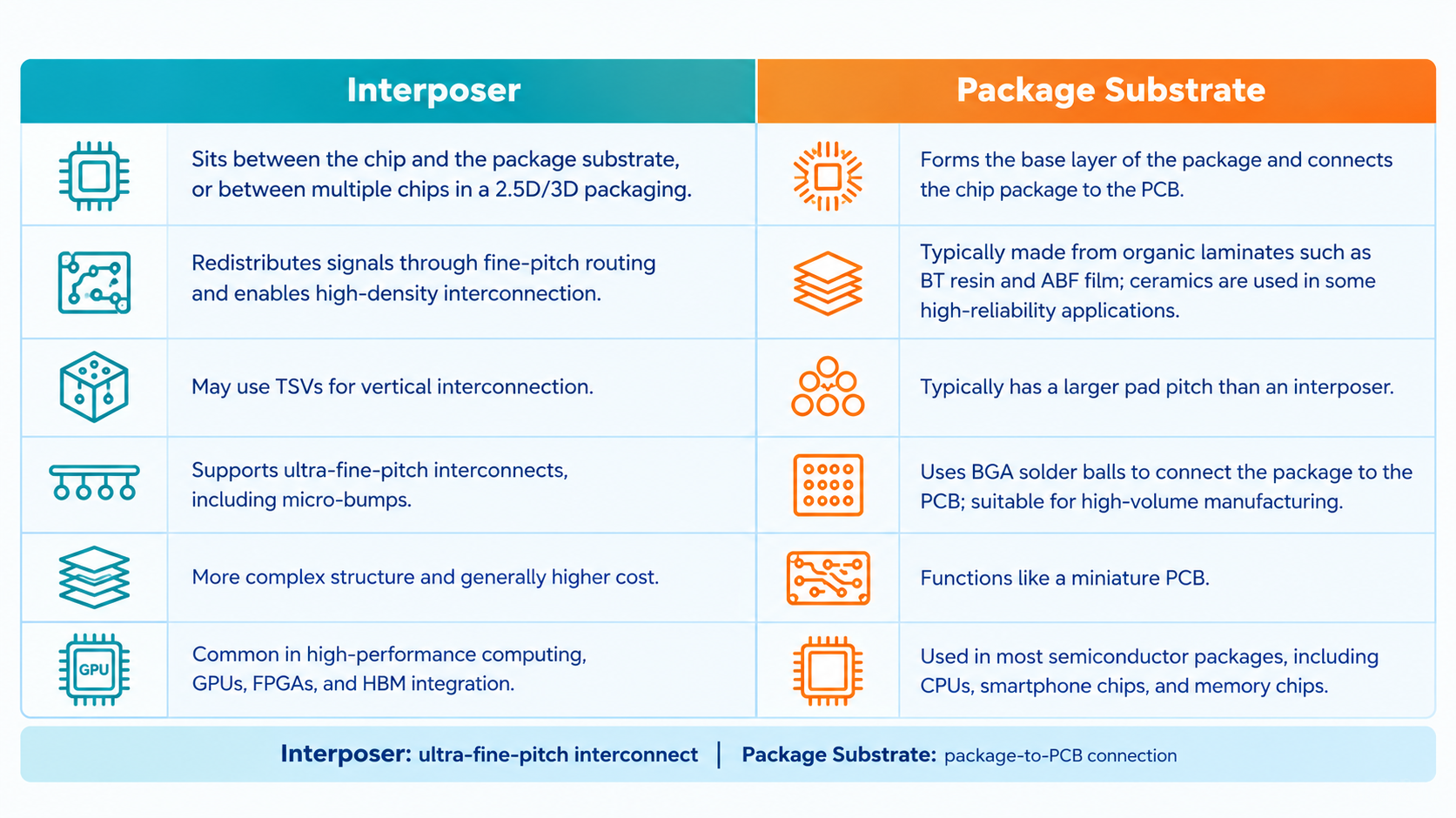
Interposers are typically thin and commonly made of silicon, glass, or organic materials. They are placed between the chip and the package substrate, or between the package and the printed circuit board (PCB). Serving as a bridge, they redistribute signal, power, and ground connections through fine-pitch routing or through-silicon vias (TSVs). Interposers enable high-density interconnection and fine-pitch routing, thereby connecting the tiny pads on an integrated circuit (IC) to the larger, manufacturable pads on a PCB.
In advanced packaging, interposers also allow multiple chips (such as logic chips and memory chips) to be mounted side by side within the same package. Such packages are very common in high-performance computing, for example, graphics processing units (GPUs) and field-programmable gate arrays (FPGAs). Interposers help handle the differences in routing pitch and dimensions between chips and substrates, thereby reducing stress and improving assembly reliability. By shortening interconnect lengths and increasing routing density, interposers can enhance electrical performance (such as improving signal integrity and reducing latency) and, to some extent, improve heat dissipation.
Interposers can be broadly classified into three categories:
· Silicon interposers: employing TSVs, enabling extremely fine pitch and high-performance interconnection;
· Glass interposers: relatively lower cost with good dimensional stability;
· Organic interposers: made from advanced laminate materials, lower cost but with routing density inferior to silicon interposers.
In short, interposers are critical components that provide a high-density interconnect layer and transition support between chips and substrates, and are of great significance to advanced packaging of modern semiconductor devices.

2 Evolution of Interposers
With the development of semiconductor manufacturing and advanced packaging technologies, the definition of "interposer" has been continuously evolving.
In the past, interposers typically referred to:
① A passive intermediate substrate used to redistribute I/O signals between a semiconductor chip and a larger substrate/PCB;
② Made of silicon, glass, or organic laminates;
③ Featuring fine-pitch routing, TSVs, and redistribution layers (RDL);
④ Used to address mechanical, electrical, and pitch-scaling challenges.
With the rise of 2.5D, 3D packaging, and heterogeneous integration, the role of interposers is changing, and several new types of interposers have emerged:
Passive interposers (traditional role)
These interposers are still widely used in silicon photonics, GPUs, FPGAs, and high-bandwidth memory (HBM) integration, offering high-density routing and power distribution.
Active interposers
These interposers integrate transistors, power delivery circuits, and signal conditioning logic internally. Typical functions include managing clock distribution, voltage regulation, and high-speed signal retiming. Active interposers are gaining increasing attention in the chiplet ecosystem, as chiplets from different vendors require standardized interconnection.
Organic/hybrid interposers
In cost-sensitive applications, laminate and build-up film technologies are becoming strong competitors to silicon-based solutions. To achieve moderate performance at lower cost, some approaches use TSV-free RDL fan-out interposers.
Glass interposers
Glass interposers are emerging due to their low cost, low loss, good dimensional stability, and ability to handle ultra-high-density I/O.
3 Expansion of the Term "Interposer"
The term "interposer" originally referred mainly to silicon bridges based on TSV technology. Today, the scope of the term has expanded to include RDL interposers (fan-out redistribution layers, simulating TSV-free interposers), as well as embedded bridge technologies like Intel's Embedded Multi-die Interconnect Bridge (EMIB), sometimes called "local interposers." Even wafer-level package substrates with high-density interconnects are blurring this boundary. In other words, the boundaries between "interposer," "substrate," and "advanced packaging layer" are no longer strict.
The technical reasons for the expansion of the term "interposer" mainly include:
· Chiplet architecture: Companies want to connect chips from different process nodes, foundries, or suppliers. Interposers are no longer merely "routing boards" but are becoming integration platforms.
· Heterogeneous integration: Logic, memory, analog, optoelectronic, and radio frequency (RF) modules can be integrated on the same interposer or through the same interposer.
· Power delivery and thermal management constraints: Active interposers help manage local power and heat at the package level.
4 Development of Interposers in Electronics Manufacturing
4.1 Early Stage (2000s–Early 2010s): Classic Silicon Interposers
Interposers at this stage were primarily defined as passive silicon boards with TSVs and RDL, used in 2.5D packaging where multiple chips (such as logic chips and HBM memory) are mounted on an interposer, which is then mounted on a package substrate. Typical examples include Xilinx FPGAs and AMD GPUs with HBM memory integration. In industry discourse, interposers were almost synonymous with TSV-based silicon interposers.
4.2 Development Stage (Mid-2010s): Organic and Glass Interposers
Organic interposers are made from laminates (such as ABF film and BT resin), offering lower cost and wider pitch than silicon interposers, suitable for applications with lower TSV density requirements. Glass interposers entered the research and early adoption stage, offering good dimensional stability, low electrical loss, and potential for extremely fine-pitch drilling. As a result, the term "interposer" has come to encompass multiple material types, no longer limited to silicon.
4.3 Redefinition Stage (Late 2010s–Early 2020s): Bridging and RDL Fan-Out Technologies
Fan-out RDL interposers are redistribution layers on reconstituted wafers or panels, functioning like interposers without TSVs, primarily used in advanced fan-out wafer-level packaging (FOWLP). Embedded bridges (local interposers), typified by Intel's EMIB, use small interposer "tiles" embedded only where needed, reducing cost compared to full silicon interposers. As a result, the term "interposer" has expanded to include partial/local connection platforms.
4.4 Next Generation (2020s–Future): Active Interposers
Active interposers can not only redistribute signals but also integrate active circuits, including power management (such as voltage regulators), clock distribution, and signal retiming, and may potentially be used for security or interconnect logic in the chiplet ecosystem. Related research examples include CERN, CEA-Leti, and commercial development by foundries and outsourced semiconductor assembly and test (OSAT) companies. The industry impact is that the boundaries between "substrate," "interposer," and "system-level interposer" are further blurred.
Today, the industry uses "interposer" as a broad term to refer to any component located between chips and substrates that enables high-density integration. This definition is no longer limited to passive silicon interposers with TSVs.

5 Common Ground: High-Density Interconnect (HDI) and UHDI
In advanced semiconductor packaging, substrates are in many ways similar to miniature high-density interconnect (HDI) PCBs. The laser-drilled microvias, fine lines, and multilayer build-up technologies used in substrates were originally applied in HDI PCB manufacturing. As line width/spacing requirements shrink to single-digit micrometers, substrate manufacturing is beginning to look almost identical to the most advanced PCB manufacturing technologies, only with smaller geometries and tighter tolerances. The push of PCBs toward ultra-high-density interconnect (UHDI) echoes the changes occurring in advanced packaging substrates.
5.1 Substrates and HDI Boards: Evolving on Demand
Early substrates could be manufactured using traditional processes similar to PCB fabrication. As chip I/O counts increased, substrates had to evolve, and engineers adopted technologies such as build-up methods, stacked vias, and laser drilling, which became hallmarks of HDI. Currently, high-end substrates for CPUs, GPUs, and network application-specific integrated circuits (ASICs) feature UHDI-level technical characteristics: line width/spacing below 10 µm, microvias below 50 µm, and highly controlled layer-to-layer registration. In many respects, substrate manufacturing has technically surpassed traditional HDI PCBs, and the PCB industry is striving to catch up.
5.2 Interposers and UHDI Boards: Overlapping Areas
Silicon interposers with TSVs are manufactured through semiconductor processes rather than PCB processes. However, RDL fan-out interposers (such as those used in FOWLP) and glass/organic interposers employ processes very similar to HDI PCB manufacturing, only with extremely high resolution requirements. Some in the industry even call fan-out panels "PCB-like interposers" because their tool sets and design principles (such as vias, laminates, and redistribution layers) highly overlap with advanced PCB manufacturing processes. UHDI technology directly supports the density required for chiplet interconnection, which is precisely where interposers play a role.
5.3 Manufacturing Convergence
In the past, PCB manufacturers, substrate manufacturers, and semiconductor manufacturers operated independently. However, with the development of HDI/UHDI technologies, these distinctions are gradually blurring. PCB manufacturers are investing in UHDI capabilities to support next-generation substrate production; substrate manufacturers (such as Ajinomoto, Ibiden, and Unimicron) are adopting PCB-style panel processing with higher resolution; large panels are being used for fan-out packaging, with equipment overlapping with PCB manufacturing equipment. This convergence means that the skills and processes of HDI/UHDI PCB manufacturing are directly driving the development of interposers and substrates.
6 Relationship Among Interposers, Substrates, and PCBs
6.1 Why This Matters
As the boundary between chip packaging and PCBs gradually blurs, the technologies of substrates and UHDI PCBs are becoming interoperable. In some technology roadmaps, "circuit boards" and "packaging" will merge into a single integrated platform. PCB manufacturers with UHDI expertise may find opportunities to enter the advanced packaging market, while OSAT companies and substrate manufacturers are exploring panel-scale manufacturing. UHDI technology is expected to be critical not only for PCBs but also for all interconnect platforms, including substrates, interposers, and possibly hybrid chip/board integration.
For a long time, substrates have been a specialized branch of HDI PCB manufacturing, continuously pushing finer features to keep pace with semiconductor development. Interposers, especially organic and fan-out interposers, are closely related to UHDI processes and often employ PCB-like manufacturing methods. As HDI advances toward UHDI, the distinctions among PCB, substrate, and interposer manufacturing are narrowing, foreshadowing a future in which they will form a continuum of high-density interconnect platforms.
6.2 Conceptual Clarification: An Intuitive Analogy
· Interposer = adapter/converter: fanning out ultra-fine signals from the chip;
· Substrate = foundation/carrier board: connecting the adapted signals to the entire package and to the outside world.
6.3 Key Differences
· Interposer: enables chip-to-chip or chip-to-substrate connection through ultra-fine-pitch routing;
· Substrate: enables package-to-PCB connection through larger-scale routing and mechanical support.
6.4 Impact on PCBs
As technology continues to advance, traditional definitions and the functions of substrates and interposers are becoming broader. What does this mean for PCBs? According to the information presented in this article, substrates and interposers—once connectors between PCBs and chips—are now serving as more complex interconnect carriers that in many ways parallel the traditional role of PCBs.
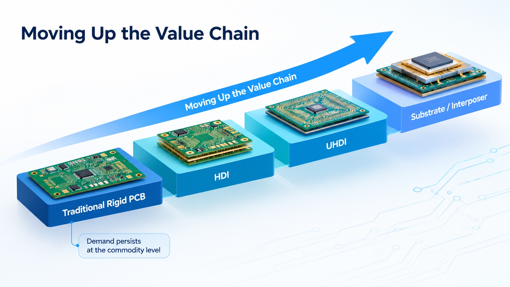
So, will both continue to exist? Or will substrate and/or interposer technologies render PCBs obsolete once certain technology boundaries are crossed? Demand for traditional rigid PCBs will not disappear entirely. For many technologies, it will remain the most economical connection option. However, as HDI gradually transitions to UHDI and high-end applications demand more advanced manufacturing capabilities, substrate and interposer manufacturing—despite requiring different equipment and materials—may become the next logical development direction for traditional PCB factories.
7 Conclusion
Interposers have evolved from classic passive silicon TSV interposers to a broad range of high-density integration platforms encompassing organic, glass, fan-out RDL, embedded bridge, and active interposers. Substrates continue to advance toward UHDI, constantly approaching and even surpassing traditional HDI PCBs in feature size and process control. As UHDI technology drives the convergence of PCB, substrate, and interposer manufacturing processes, the boundaries between the three are increasingly blurred, and they are expected to form a continuous high-density interconnect platform in the future. For the traditional PCB manufacturing industry, this is both a technological challenge and a strategic opportunity to move up the value chain.
trending news
Contact Us