




Sorry, no sales person is available right now to take your call. Pls leave a message and we will reply to you via email as soon as possible.
RF and Microwave PCB Design: A Complete Guide from Material Selection to Manufacturing Implementation
2026-10-23
With the widespread application of wireless systems in AI infrastructure, automotive radar, aerospace, satellite communications, Wi-Fi, 5G, and IoT devices, RF and microwave PCB design is becoming increasingly important. As operating frequencies rise, PCB traces are no longer equivalent to simple wires—every trace, every via, every connector, and every material becomes an integral part of the electrical system.
What Is RF and Microwave Printed Circuit Board Design?
RF and microwave PCB design focuses on circuits operating at high frequencies, where transmission line effects, impedance control, and electromagnetic behavior become critical design considerations.
Traditional low-frequency PCB design primarily treats traces as electrical connections. In RF and microwave systems, however, traces behave as controlled transmission lines that must maintain constant impedance and minimize reflection and loss.
Many modern applications operate across multiple frequency bands, such as:
· 915 MHz
· 2.4 GHz
· 5 GHz
· 24 GHz
· 28 GHz
· 39 GHz
· 77–81 GHz
These frequencies are widely used in wireless networks, radar, satellite communications, automotive sensing, and millimeter-wave systems.
Why Is PCB Material So Important in RF Design?
PCB materials directly affect signal loss, impedance stability, thermal performance, and manufacturability. Two of the most important material properties are:
Dielectric Constant (Dk)
Dk affects signal propagation velocity and impedance. A stable Dk helps maintain predictable RF performance across frequency and temperature variations.
Dissipation Factor (Df)
Df measures the degree to which signal energy is lost as heat. Low-Df materials reduce insertion loss and improve signal integrity at high frequencies.
Standard FR-4 is suitable for some low-frequency RF applications, but high-frequency systems typically require:
· Low-loss FR-4 hybrid materials
· Hydrocarbon ceramic laminates
· PTFE-based materials
These materials provide lower insertion loss and more stable RF performance.
What Transmission Line Structures Are Used in RF Circuit Boards?
RF PCB layout relies on controlled-impedance transmission lines. Common structures include:
Microstrip
Microstrip routes signals on the outer layer above a reference plane. It is relatively easy to route and probe, but is more susceptible to impedance variations caused by environmental factors.
Grounded Coplanar Waveguide (GCPW)
GCPW adds ground copper alongside the signal trace to improve field confinement, isolation, and emission performance.
Stripline
Stripline places the signal trace between reference planes within the PCB stackup, providing strong shielding and lower crosstalk, but it requires tighter manufacturing control and is less convenient for debugging.
The choice of the optimal structure depends on frequency, routing density, isolation requirements, and manufacturability.
Which Layout Practices Improve RF Performance?
RF PCB layout has a major impact on system performance. Key best practices include:
· Maintain a continuous ground plane
· Keep RF traces short and direct
· Avoid interruptions in high return-current paths
· Place via fences around sensitive RF structures
· Carefully design connector launch structures
· Separate noisy digital circuits from sensitive RF sections
At higher frequencies, even minor layout discontinuities can affect insertion loss, return loss, and radiation performance.
How Do Vias Affect RF PCB Performance?
Vias introduce inductance and discontinuities that can degrade RF performance if not properly controlled. Common strategies include:
· Back-drilling short stub vias
· Using blind or buried vias
· Adding stitching vias at layer transitions
· Minimizing unnecessary layer changes
At microwave frequencies, via transitions should generally be modeled using electromagnetic simulation tools.
How Are RF and Microwave PCBs Tested?
Testing verifies that the PCB performs correctly at its operating frequencies. Common RF test equipment includes:
· Vector network analyzers (VNA)
· Spectrum analyzers
· Time-domain reflectometers (TDR)
Engineers use these tools to measure:
· Return loss
· Insertion loss
· Impedance discontinuities
· Harmonic and spurious emissions
· Group delay and phase behavior
Proper calibration and fixture design are essential for obtaining accurate measurement results.
Which IPC Standards Apply to RF PCB Design?
IPC standards commonly referenced in RF and microwave PCB manufacturing include:
· IPC-2221
· IPC-2226
· IPC-6012
· IPC-6018
· IPC-TM-650
These standards help define design requirements, material properties, manufacturing quality, and test methods for RF and microwave PCBs.
Why Manufacturing Precision Matters More at Microwave Frequencies
At microwave frequencies, manufacturing tolerances directly affect electrical performance, involving factors such as:
· Copper thickness
· Trace width variation
· Dielectric thickness
· Copper foil roughness
· Etch compensation
All of these factors affect impedance and insertion loss. RF PCB manufacturing therefore requires close collaboration between design and manufacturing teams. Controlled-impedance planning, stackup verification, and DFM reviews should be carried out early in the project.
Conclusion
Successful RF and microwave PCB design requires a combination of solid electrical engineering, controlled PCB layout, material selection, and rigorous manufacturing.
The most reliable RF PCB process should:
· Define electrical requirements first
· Select materials based on loss and stability
· Adopt controlled layout
· Verify performance through measurement
· Align design and manufacturing early
As wireless systems continue to evolve toward higher frequencies and tighter tolerances, early collaboration between engineering and manufacturing is increasingly important for achieving predictable RF performance.
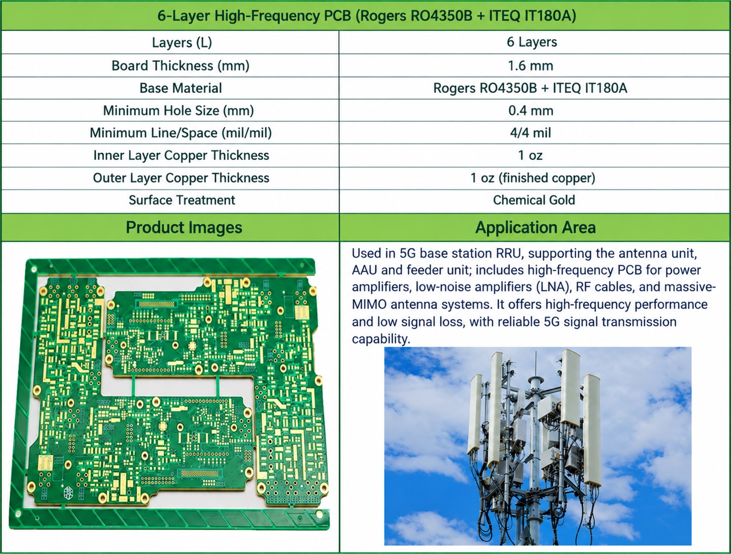
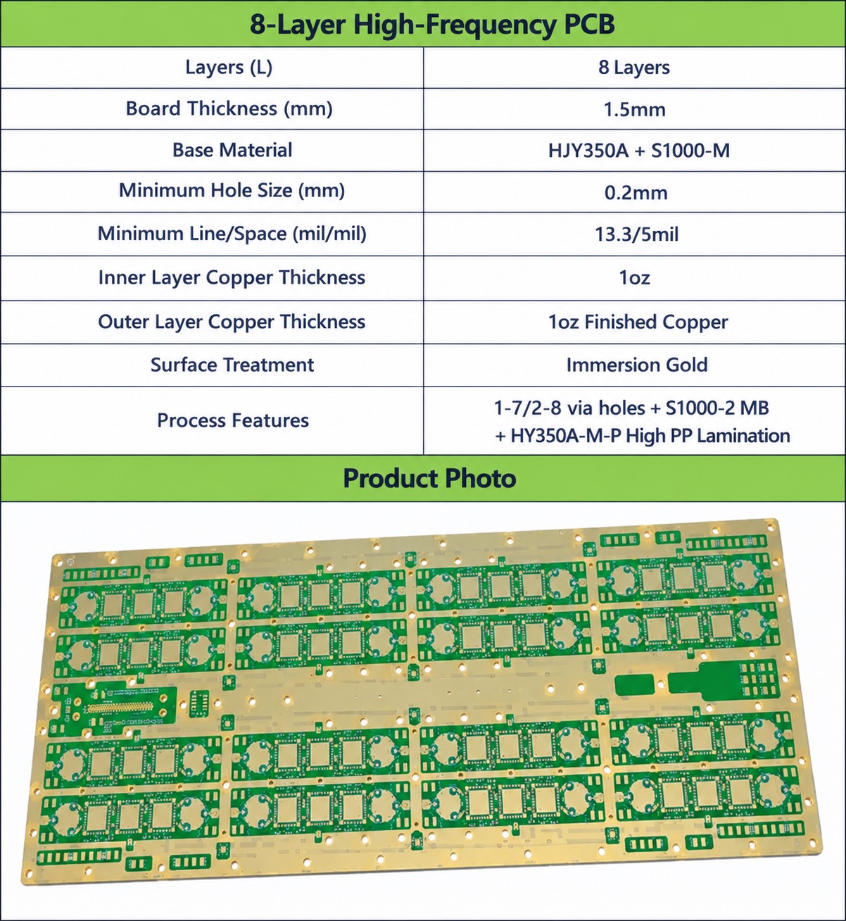
KINJI GROUP High-Frequency Board Product Showcase

trending news
Contact Us