


Sorry, no sales person is available right now to take your call. Pls leave a message and we will reply to you via email as soon as possible.
Why Design Segmented Gold Fingers on Optical Module PCBs?
2026-10-16
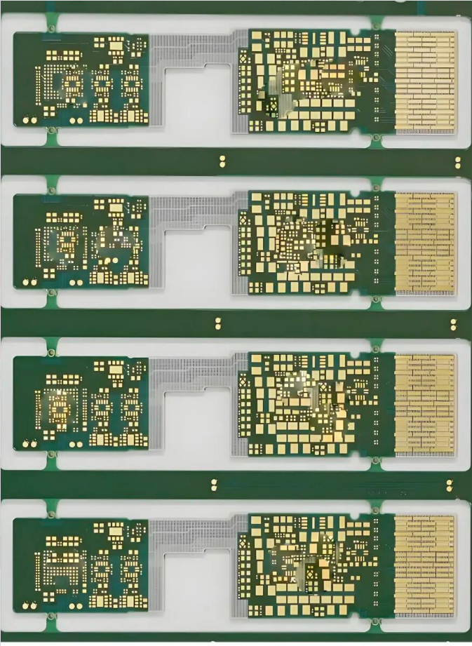
Optical modules are opto-electronic conversion devices for high-speed communications. A typical module consists of optical components, electrical chips, PCB, mechanical housings and thermal structures. The edge of the PCB that plugs into switches or servers features gold-plated contact areas, commonly called gold fingers.
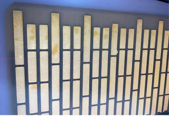
Segmented gold fingers are not merely cosmetic. Contact zones are partitioned and isolated by electrical functions. Varying contact pin lengths are used to manage power-up / power-down timing. This design balances signal integrity, power integrity, hot-plug sequencing, mechanical mating and manufacturability for mass production.

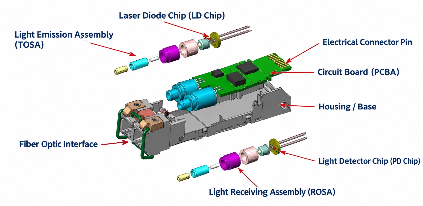
(Figure: Diagram — Edge segmented gold fingers on optical module PCB)
1. Core characteristics of optical modules
🔹 High-speed & high-frequency Data rates have evolved from 1G/10G, 25G/100G to 200G/400G/800G and beyond, creating strict requirements for signal integrity, power integrity and high-speed interconnection.
🔹 Mixed optoelectronic design Combining photonics and electronics, integrating lasers, modulators, photodiodes, DSP, CDR, driver and TIA chips. Design and testing require cross-domain expertise.
🔹 High density & compact form factor Standard packages include SFP, SFP28, QSFP, QSFP-DD and OSFP. High-speed circuits, optical components and thermal structures must fit in limited space.
🔹 Thermal-sensitive Rising power consumption from high-speed ICs and optoelectronic components makes thermal resistance, temperature rise and operating temperature critical design factors.
🔹 High reliability requirements Long-term continuous operation in telecom equipment requires validation for temperature cycling, humidity, mechanical stress, plug endurance and high-speed electrical performance.
🔹 High standardization Mechanical dimensions, electrical interfaces, management and optical interfaces follow specifications from MSA, IEEE and OIF. Designs must maintain cross-vendor compatibility.
Note: Chip architecture, optical design, power consumption and manufacturing challenges differ significantly for modules of varying speed grades and packages. Not all modules follow the same configuration.

2. Why use segmented gold fingers?
Segmentation partitions and isolates contacts by electrical function, while optimizing high-speed performance, power return paths and hot-plug timing.
· Functional separation: High-speed differential pairs, power, ground and low-speed management signals are assigned to dedicated contact zones.
· Reduce crosstalk: Proper arrangement of signal, power and ground contacts suppresses electromagnetic coupling between adjacent high-speed traces.
· Improve signal integrity: Differential pairs require consistent impedance and controlled return paths. Placement, length, spacing and reference ground design directly impact SI performance.
· Hot-plug sequencing: Staggered pin lengths define connection order: ground first, then power, finally signal. Reverse sequence for removal. This avoids unexpected electrical states during hot swapping. Always refer to official interface specifications.
· Enhanced contact reliability: Contacts have different requirements for contact resistance, wear resistance and plating quality. Gold finger construction and surface finish must match the mating connector.
In engineering terms: segmented gold fingers use functional zoning, geometry and staggered pin lengths to satisfy high-speed electrical performance, power/ground return paths and hot-plug sequencing at the same time.

3. Key manufacturing challenges
The difficulty lies in stable mass production while maintaining high density, high speed and reliability.
· Dimensional precision: Line width, spacing, pin length, chamfering and board edge position must be tightly controlled. Tolerance stack-up from etching, plating and routing may shift contact positions and degrade high-speed channel performance.
· Gold plating quality & plug endurance: Plating thickness, uniformity, adhesion and surface defects (scratches, pits, exposed copper) must be controlled to stabilize contact resistance after repeated plugging. Current distribution and fixture contacts during plating may cause uneven gold coverage.
· Process window for segmented zones: Mixed pin lengths, isolated zones and fine spacing demand strict control over pattern accuracy, plating uniformity and routing tolerance, with narrower process windows than standard continuous gold fingers.
· Consistency for high-speed performance: At 100G/400G/800G+, PCB production must guarantee impedance, insertion loss and return loss. Variations in dielectric thickness, Dk, copper weight and undercut directly affect high-speed metrics, requiring linked control between PCB process capability and SI specs.
· Multi-material & multi-process coordination: Optical assembly, chip bonding, connectors and thermal materials bring different CTE and thermal/mechanical properties. Assembly stress or board warpage may compromise long-term thermal reliability.
· High-density assembly & yield: Compact size and dense components couple SMT, precision bonding, optical coupling and testing. Minor process deviations may only surface during optical or high-speed electrical testing. Yield management, failure analysis and test coverage are vital for mass production.
Summary
The core challenge of optical module manufacturing is integrating high-speed electrical performance, optical performance, thermal control, mechanical fit and long-term reliability within a small form factor, and translating tight design tolerances into stable mass production.
Segmented gold fingers are designed for interface partitioning, signal integrity, power return and hot-plug sequencing. Manufacturers must tackle dimensional accuracy, plating durability, high-speed impedance/loss control and assembly yield. Final segmentation layout, pin length and plating specs depend on package type, connector definition and industry standards including MSA, IEEE and OIF.
trending news
Contact Us