

Sorry, no sales person is available right now to take your call. Pls leave a message and we will reply to you via email as soon as possible.
Substrate-Like PCBs (SLP): The Interconnect Technology Reshaping Compact Next-Generation Electronics
2026-10-14
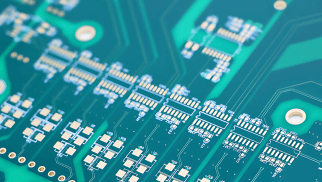
The relentless pursuit of smaller, higher-performance electronics continues to push conventional high-density interconnect (HDI) printed circuit boards to their design limits. Across consumer wearables, smartphones, slim computing hardware and space-constrained automotive electronics, Substrate-Like PCBs (SLP) have emerged as a critical intermediate technology, bridging the performance gap between advanced HDI boards and specialized IC package substrates.
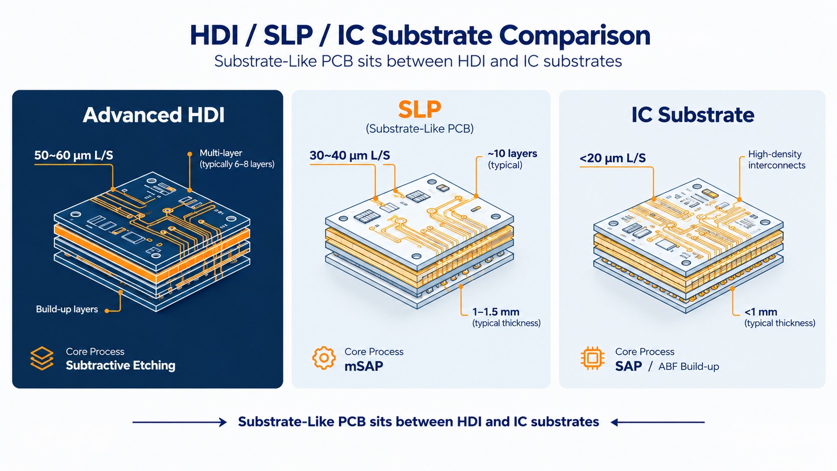
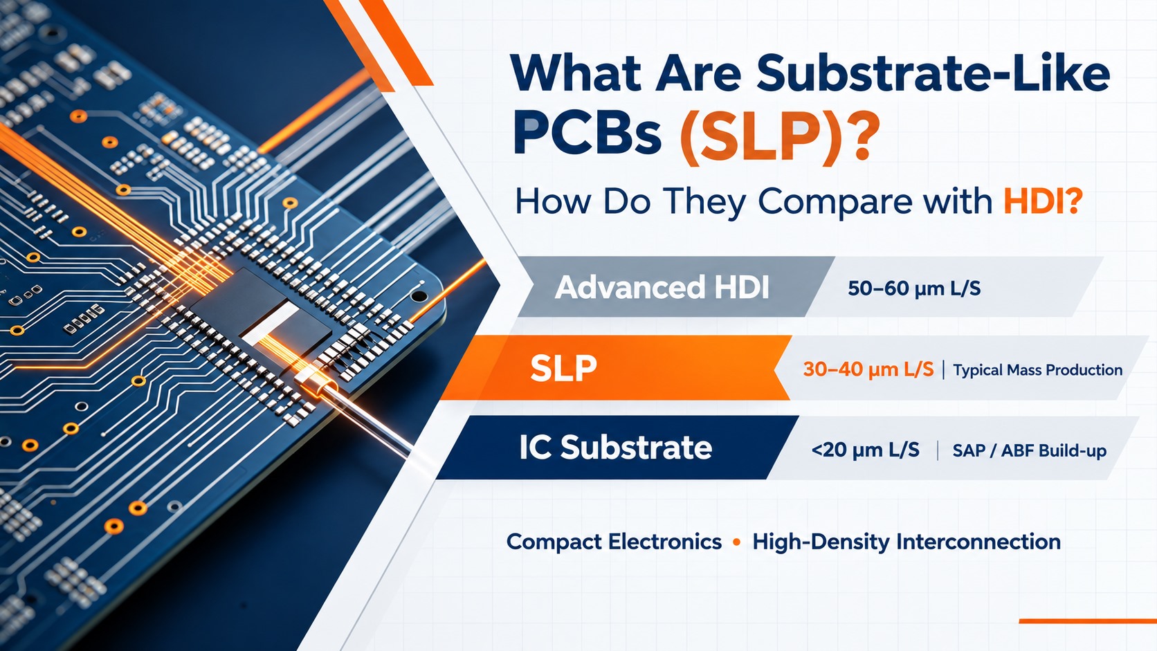
SLP retains the panel-based production and board-level component assembly advantages of traditional PCBs, while adopting manufacturing technologies originally developed for IC substrates to enable ultra-fine circuit geometries. While laboratory-grade SLP processes can reach 25–30 μm line width and spacing, stable mass production typically operates within the 30–40 μm range. Unlike IC substrates, which are built primarily for die-to-package interconnection, SLP can directly mount both active and passive electronic components at board level. This unique combination makes it well suited for compact devices requiring high circuit density.
Core Manufacturing Characteristics
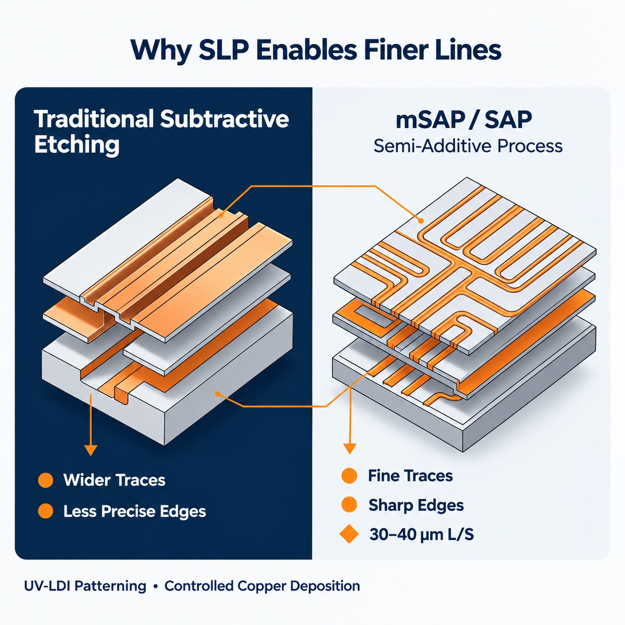
The ultra-fine wiring capability of SLP relies on two foundational technologies: UV Laser Direct Imaging (UV-LDI), and Semi-Additive Processing (SAP) or Modified Semi-Additive Processing (mSAP).
UV-LDI delivers high-precision pattern transfer required for ultra-fine traces. SAP and mSAP differ from traditional subtractive etching used on standard HDI boards. Instead of removing excess copper from a full copper foil layer, these additive processes build copper conductors through controlled deposition, resulting in sharp, clean conductor edges that support extremely fine feature sizes.
Typical SLP stack-ups feature approximately 10 layers, with finished board thickness around 1–1.5 mm, close to the physical dimensions of many IC carrier substrates.
Critical Performance Considerations
Thermal management becomes a primary design challenge as components are packed tightly into miniaturized hardware. SLP utilizes high thermal conductivity substrate materials to draw heat away from processors and other hot components. In many product designs, thermal interface materials connect the SLP to the device enclosure, turning the product casing into a passive heat dissipation structure.
Coefficient of thermal expansion (CTE) matching represents another key reliability factor. When the substrate, solder joints and mounted chips expand and contract at different rates under temperature cycling, accumulated mechanical stress eventually causes hardware failures. SLP material selection is carefully optimized to minimize CTE mismatch and improve long-term reliability under repeated thermal cycles.
For high-speed signal designs, SLP construction uses thin dielectric layers, which makes the dielectric constant (Dk) of the substrate material highly influential on signal behaviour. Low-Dk dielectrics are preferred; they allow slightly wider traces while maintaining target impedance, simplifying manufacturability for fine-pitch high-speed circuits.
Benefits and Practical Trade-offs
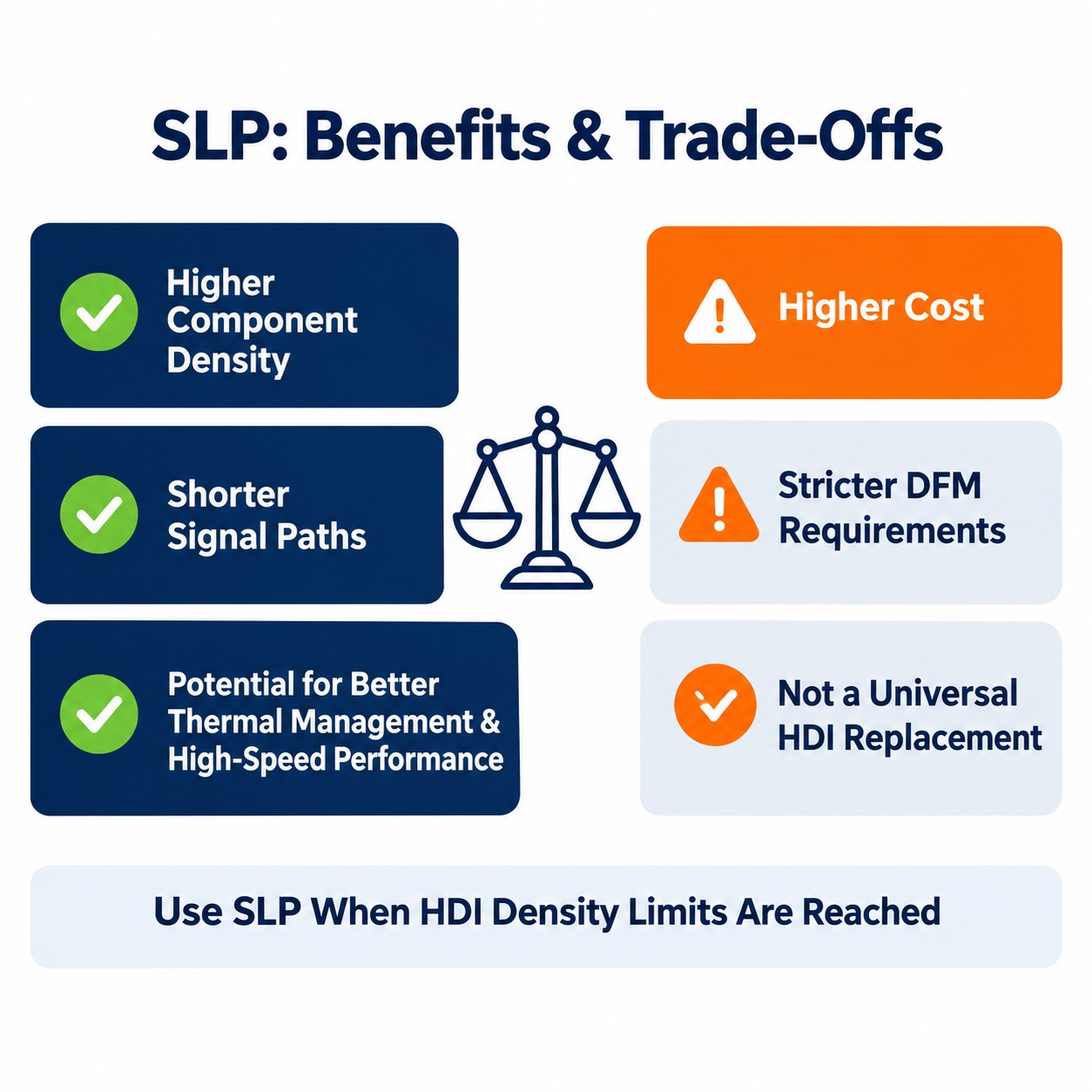
SLP delivers major advantages for miniaturized electronic systems. Compared with advanced HDI technology, designers can fit roughly twice the number of components within the same board footprint, enabling thinner and lighter end devices. Shorter interconnect traces reduce signal loss and power consumption, supporting faster high-speed data transmission. The advanced fabrication processes also achieve tighter dimensional tolerances, lowering manufacturing defect risks and improving long-term hardware durability.
Even so, SLP is not a universal upgrade solution and comes with notable limitations. Its production cost is higher than advanced HDI. The specialized production requirements create a smaller supplier base and impose stricter DFM rules, increasing upfront design effort. For applications requiring feature sizes below 20 μm, IC substrates remain necessary, as SLP cannot fully replace dedicated packaging substrates. Industry design best practice suggests that engineers should continue selecting HDI when their design requirements fit within HDI geometry limits. SLP should only be adopted once HDI density capacity is exhausted.
Industry Applications
SLP technology finds adoption in product categories where both compact physical size and high electrical performance are mandatory. These include smartphones, tablets, smartwatches and other wearables, slim laptops and ultrabooks, space-limited automotive electronics, miniaturized industrial IoT sensors and compact high-performance industrial electronic systems.
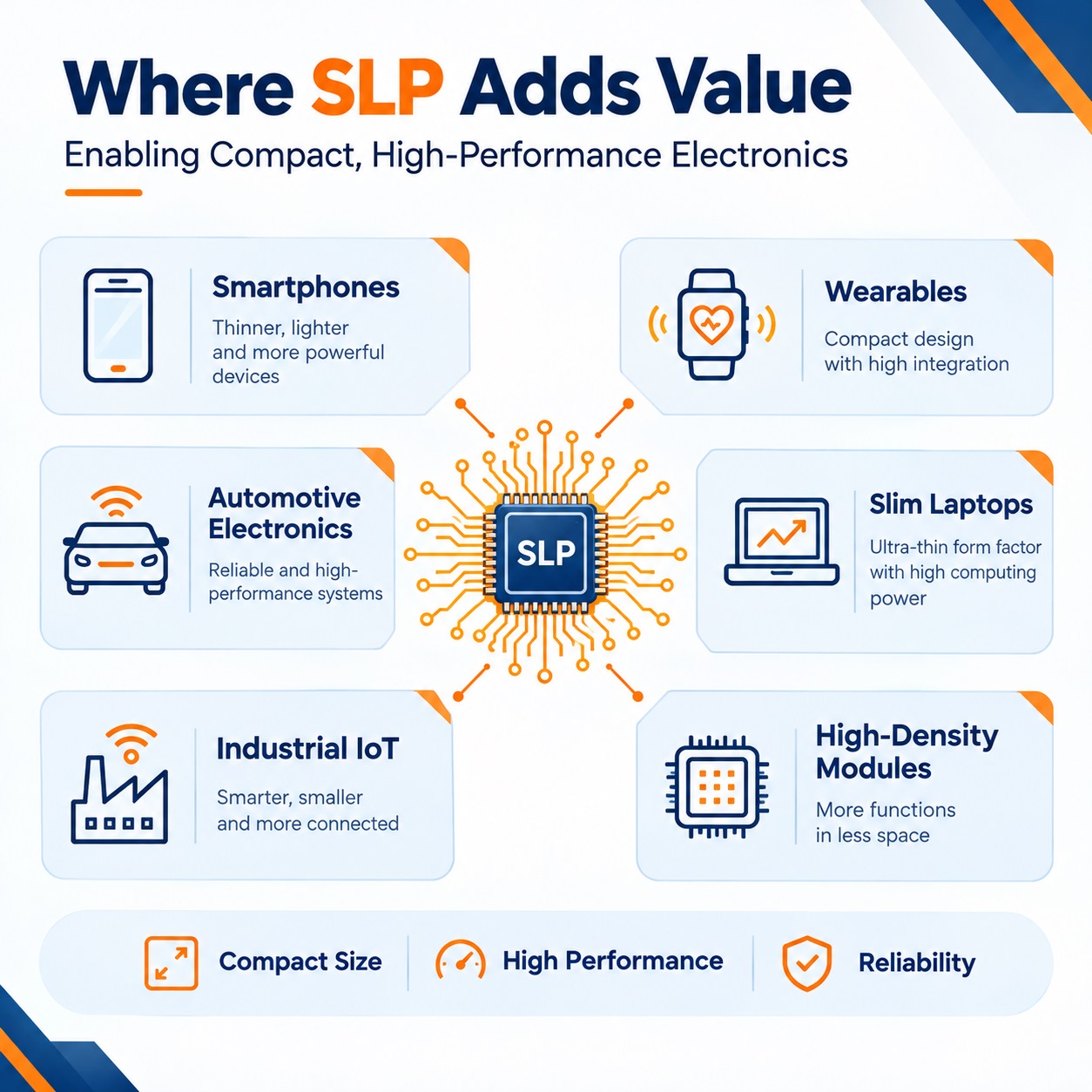
As electronic hardware continues toward miniaturization and higher computing power, SLP adoption will keep expanding for density-critical projects. At the same time, HDI will remain a cost-effective mainstream interconnect solution for the majority of electronic hardware designs.
trending news
Contact Us