


Sorry, no sales person is available right now to take your call. Pls leave a message and we will reply to you via email as soon as possible.
How to Reduce Ceramic PCB Manufacturing Costs? A Step-by-Step Embedded Process Guide
2026-10-10
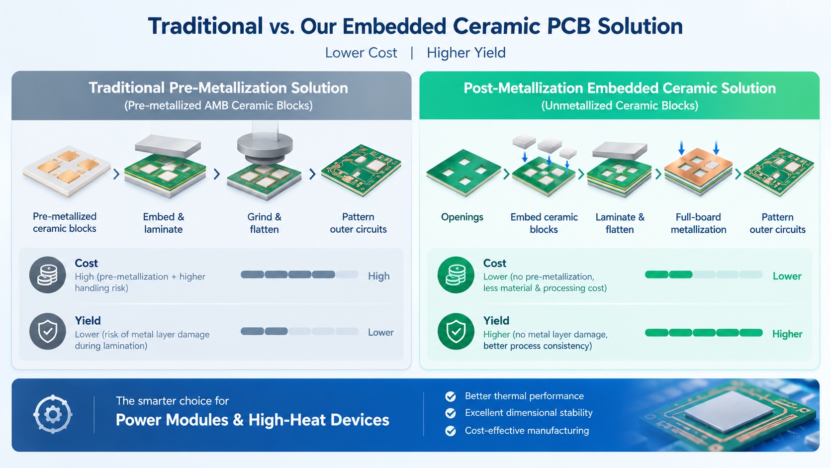
To improve the insulation and heat dissipation performance of PCBs, ceramics can be embedded into the PCB substrate. Ceramics have a low coefficient of thermal expansion (CTE), and embedding them also helps improve PCB dimensional stability, meeting the requirements of high-precision surface-mount components. Unlike the process of directly embedding pre-metallized active metal brazed (AMB) ceramic substrates, this article introduces a method for manufacturing ceramic-embedded PCBs: embedding ceramic blocks first, then metallizing the entire board in a single step. Compared with using pre-metallized ceramic blocks, this approach can reduce costs and make it easier to control the quality of ceramic-embedded PCBs.

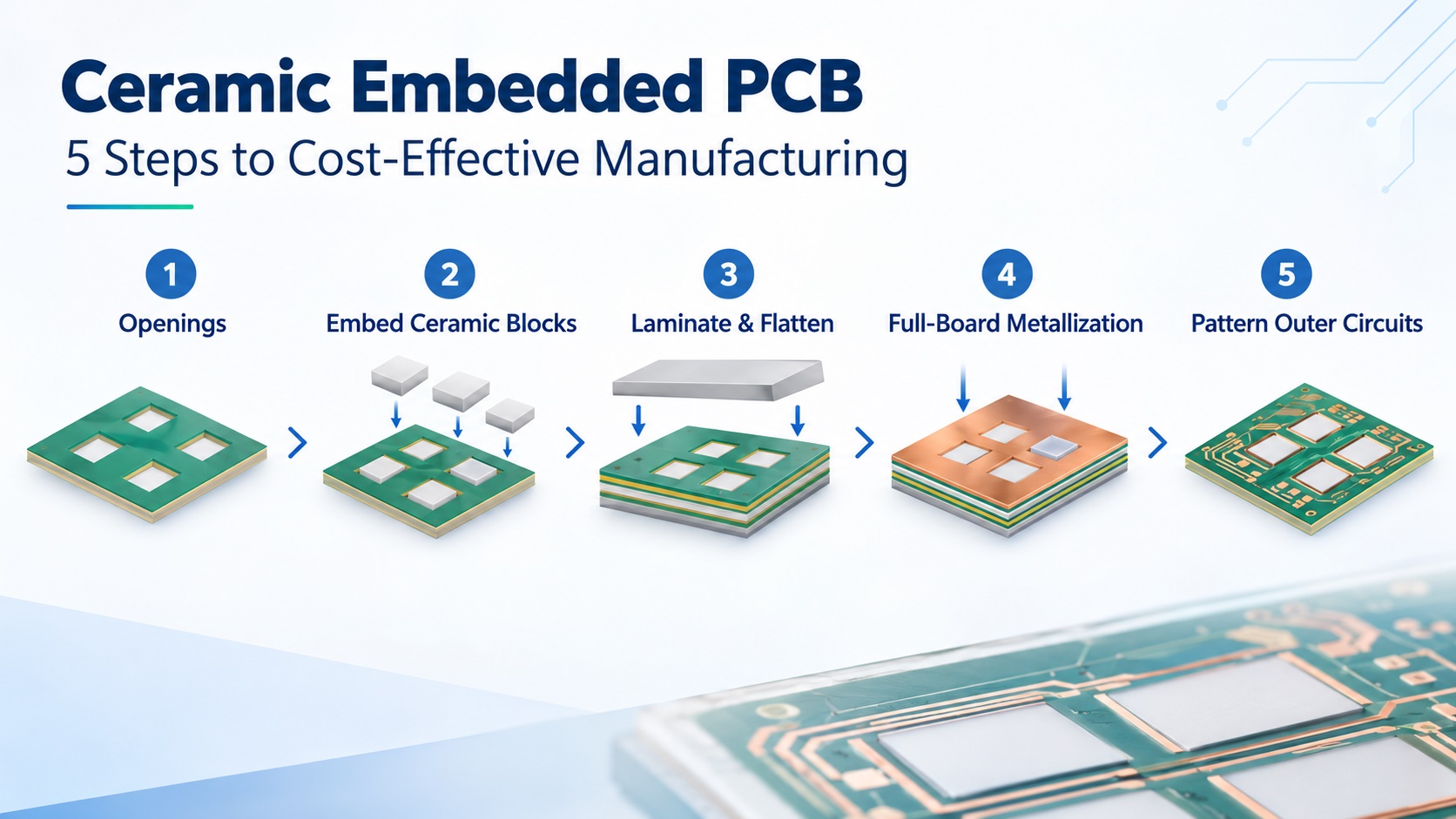
The specific process flow is as follows:
1. Inner-layer substrate pretreatment and lamination with window openings
Double-sided copper-clad laminate (CCL) is used. Before lamination, inner-layer patterning is completed: film lamination, exposure, development, and etching are carried out in sequence to obtain the inner-layer circuitry. Then, the layers are stacked in the order of "substrate—prepreg—substrate," with the inner-layer patterns facing the interior of the stack. After stacking is completed, window openings are made at predetermined positions to form cavities for placing ceramic blocks.
2. Embedding non-metallized ceramic blocks
Ceramic blocks without metal layers are placed into the window openings. The ceramic blocks can be made of one or more materials such as alumina, aluminum nitride, or low-temperature co-fired ceramic (LTCC). The ceramic blocks are slightly smaller than the window openings to leave assembly clearance and facilitate subsequent prepreg flow filling.
3. Lamination and grinding/flattening
The stack is laminated. During lamination, the prepreg melts and flows under heat, bonding the upper and lower substrates and filling the gaps between the ceramic blocks and the window openings. After lamination, the board surface is ground/polished flat so that the ceramic block surfaces are flush with the outer surfaces of the substrate, ensuring flatness for subsequent metallization and pattern fabrication.
4. Full-board surface metallization
The flattened board is metallized. First, a conductive seed layer is prepared by vapor deposition (such as physical vapor deposition, PVD), followed by copper electroplating to form an electroplated copper layer approximately 10–50 μm thick, so that a continuous metal layer is formed simultaneously on both the substrate surface and the ceramic block surfaces. If necessary, the board surface can be cleaned, activated, or roughened before metallization to improve coating adhesion.
5. Fabrication of outer-layer circuit patterns
The electroplated copper layer is subjected to film lamination, exposure, development, and etching in sequence to fabricate outer-layer circuit patterns, ultimately yielding a finished ceramic-embedded PCB.
In this method, the entire board is metallized in a single step after the ceramic blocks are embedded and flattened. Since the ceramic blocks do not need to be pre-metallized before embedding, material and processing costs can be reduced, and damage to pre-metallized ceramic blocks that may occur during embedding and lamination can be minimized, which helps improve the process consistency and quality controllability of ceramic-embedded PCBs.

trending news
Contact Us