


Sorry, no sales person is available right now to take your call. Pls leave a message and we will reply to you via email as soon as possible.
What is a "plugging vias" in PCB? Why is it necessary to do this? How is it accomplished?
2026-06-03
The through holes play the role of connecting circuits and facilitating the conduct of electricity. The development of the electronics industry has also promoted the development of PCBs, and has also raised higher requirements for the manufacturing process of printed boards and surface mount technology. The via hole filling process has emerged accordingly, and it should meet the following requirements:
(1) The conductive holes only need to have copper inside; the solder mask can be used or not used as desired.
(2) The inner part of the through-hole must contain tin and lead, and it must have a certain thickness requirement (4 microns). There must be no soldering flux ink entering the hole, as this could cause tin beads to be trapped inside the hole.
(3) The through holes must be filled with solder mask ink and should be non-transparent. There should be no solder rings, solder beads or any other flatness requirements.
As electronic products continue to evolve towards the "light, thin, short, and small" direction, PCBs are also moving towards higher density and greater complexity. As a result, there are a large number of SMT and BGA PCBs. When customers assemble components, they require blind vias, and there are mainly five purposes for this:
(1) To prevent short circuits caused by solder penetrating the component surface through the through-holes during the over-temperature wave soldering process of PCB; especially when the through-holes are placed on the BGA pads, it is necessary to first fill the holes and then perform gold plating treatment, which is conducive to the BGA welding.
(2) Prevent the presence of soldering agent in the through holes;
(3) After the surface mounting and component assembly of the electronic factory are completed, the PCB needs to be evacuated in the testing machine to create a negative pressure before the process can be completed:
(4) Prevent the surface solder paste from flowing into the holes, which could cause false soldering and affect the assembly process;
(5) Prevent the popping out of solder beads during over-wave soldering, which could cause short circuits.
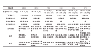
Plugging holes are divided into resin filled holes and electroplated filled holes.
Resin hole filling: Use solvent-free (without Solvent) ink to fill the holes. This not only solves the problem that regular ink is difficult to fill completely, but also reduces the occurrence of "cracks" caused by heat in the ink. It is typically used for holes with relatively large diameters in both the horizontal and vertical directions.
The advantages of resin plugging hole:
For the vias on the multilayer BGA, using resin to fill the holes can reduce the distance between the holes and solve the problems related to wires and wiring.
2. The through-holes in the inner HDI layer can resolve the contradiction between the thickness control of the dielectric layer during the bonding process and the filling design of the inner HDI through-holes.
3. The through holes with a thicker board thickness can enhance the reliability of the product;
4. In the PCB manufacturing process where resin is used to fill holes, this is often the case for BGA components. Because traditional BGA may route signals from one pad to another through vias on the surface, but if the BGA is too densely packed and the vias cannot be routed out, then the via can be directly drilled from the pad to another layer for signal routing, and the hole can be filled with resin and copper plated to become a new pad, which is commonly known as the VIP process (via in pad). If only vias are made on the pad without using resin to fill the holes, it is prone to cause tin leakage, resulting in short circuits on the backside and empty soldering on the front side.
The process of making through-holes in PCB resin involves drilling, electroplating, filling the holes, baking, and grinding. After drilling, the holes are plated through. Then, the resin is filled and baked. Finally, the holes are ground smooth. The ground resin, since it does not contain copper, requires another layer of copper to be plated on it to turn it into a PAD. All these processes are carried out before the original PCB drilling process, that is, the holes to be filled are processed first, and then other holes are drilled according to the normal process.
If the holes are not properly sealed and there are air bubbles inside, when the board passes through the soldering furnace again, it may burst. However, if there are air bubbles during the hole-sealing process, during the baking process, the bubbles will push out the resin, causing one side to be concave and the other side to be protruding. At this point, defective products can be identified. And boards with air bubbles do not necessarily burst because the main cause of bursting is moisture. Therefore, for newly manufactured boards or those that have undergone baking during the loading process, generally speaking, bursting is not likely to occur.
Electroplated hole filling: Currently, this process is carried out by utilizing the properties of additives to control the growth rate of copper in different parts, thereby enabling the filling of holes. It is mainly applied in the production of continuous multi-layer stacked holes (blind hole manufacturing process) or in high-current designs.
The advantages of electroplating hole filling:
It is conducive to designing overlapping holes and holes on the plate.
2. Improving electrical performance is beneficial for high-frequency design;
3. Helps with heat dissipation;
4. The hole sealing and electrical connection are completed in one step.
5. The blind holes are filled with copper electroplating, which provides higher reliability and better conductivity than conductive adhesives.
trending news
Contact Us