





Sorry, no sales person is available right now to take your call. Pls leave a message and we will reply to you via email as soon as possible.
Optimizing Plating Thickness for Enhanced PCB Durability and Performance
2026-09-09
In real-world PCB applications, a puzzling phenomenon often occurs: two boards that look identical and operate under the same conditions can exhibit vastly different service lives. One withstands thousands of thermal cycles without issue, while the other develops cracked vias within just a few months. The root cause frequently traces back to plating thickness. This seemingly minor metallic layer is not only responsible for current conduction, pad protection, and via interconnection, but also directly determines the long-term reliability of the PCB.
Plating thickness affects copper trace current-carrying capacity, solder joint formation quality, and connector durability through repeated mating cycles. Yet, this parameter is often overlooked during the design phase. This article starts with the fundamental concepts of plating thickness, systematically examines its impact on PCB performance, reviews industry standards, highlights quality control essentials, and incorporates Kinji Group's technical expertise in precision plating to provide actionable optimization recommendations for designers.
Definition and Classification of Plating Thickness
Plating thickness refers to the thickness of the metallic layer deposited on the PCB surface during manufacturing, typically expressed in micrometers (µm). Requirements vary across different areas of the board, including:
· Hole wall copper: The copper layer inside drilled vias and through-holes, enabling interlayer electrical connections.
· Surface copper: The electroplated copper added to outer-layer traces and pads.
· Surface finish: Protective coatings such as gold, tin, silver, or OSP that preserve solderability and prevent copper oxidation.
· Edge connector plating: Hard gold layers on gold fingers, designed for high-wear resistance during repeated insertions.
Each layer serves a distinct purpose, and improper thickness control can directly lead to poor solder joints, open circuits, and other failures.
Copper Plating vs. Surface Finish Plating
Copper plating is an electrolytic deposition process that builds the conductive backbone of the PCB. Its thickness determines current-carrying capacity and via fatigue resistance. Outer-layer copper foil is typically plated up from a thin base to a finished weight of 1 oz (~35 µm) or 2 oz (~70 µm). In contrast, surface finish plating is a thin protective layer, usually measured in nanometers to a few micrometers, designed to prevent copper oxidation and ensure solderability during assembly.
How Plating Thickness Affects PCB Performance
Plating thickness directly influences the electrical, thermal, and mechanical behavior of the board:
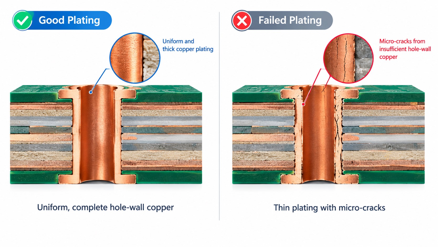
· Current-carrying capacity and reliability: Thicker copper layers carry more current with lower temperature rise. IPC-2221 curves show that 1 oz and 2 oz copper have distinctly different current capabilities at the same trace width. Insufficient hole wall copper thickness can lead to micro-cracks during thermal cycling, eventually causing open circuits. IPC-6012 specifies minimum average hole wall copper of 20 µm for Class 2 boards and 25 µm for Class 3 boards.
· Signal integrity: At high frequencies (>100 MHz), variations in copper thickness alter impedance and may cause signal reflections. The skin effect makes GHz-frequency signals particularly sensitive to plating uniformity.
· Thermal management and mechanical strength: Copper is an excellent thermal conductor. Thicker copper layers and well-plated thermal vias reduce thermal resistance and help control junction temperatures. Meanwhile, a robust hole wall copper barrel acts like a rivet, strengthening the board against shear stress from flexing and thermal expansion—especially critical in thick boards or those with high aspect ratios.

Industry Standards and Recommended Thickness Values
IPC-6012 (rigid boards) and IPC-4552/4556 (surface finishes) are the primary reference standards for plating thickness. Common thickness ranges are as follows:
· Hole wall copper (Class 2): Average ≥20 µm, minimum local ≥18 µm (suitable for most consumer electronics).
· Hole wall copper (Class 3): Average ≥25 µm, minimum local ≥20 µm (required for automotive, medical, aerospace, and other high-reliability applications).
· Outer conductor: For 1 oz base copper, the finished minimum total thickness shall reach 46 µm; for 2 oz base copper, 76 µm. Designing to only 35 µm or 70 µm may result in insufficient current margin.
· Hard gold for edge connectors: Standard ≥0.76 µm (30 µin); for high-wear scenarios, ≥1.27 µm (50 µin) is recommended.
· HASL: Approximately 1–25 µm (uneven, cost-effective).
· ENIG nickel layer: 3–6 µm; gold layer: 0.05–0.1 µm (suitable for fine-pitch BGAs).
· OSP: Approximately 0.2–0.5 µm (single reflow assembly).
· Immersion silver: Approximately 0.1–0.3 µm (RF applications).
· Immersion tin: Approximately 0.8–1.2 µm (press-fit applications).
For high-reliability, high-current designs, it is advisable to adopt Class 3 hole wall copper, 2 oz or heavier copper, optimized thermal via layouts, and trace width adjustments per IPC-2221 guidelines.
Key Factors Affecting Plating Quality
Achieving uniform and consistent plating thickness depends on precise control of multiple process parameters:
· Current density distribution (edge effect)
· Bath chemistry (copper, acid, and additive concentrations)
· Pulse or periodic-reverse plating (enhances deposition into high-aspect-ratio holes)
· Anode-to-cathode geometry and fixturing
· Filtration and temperature control (prevents rough or nodular deposits)
Deviation in any of these parameters can result in thin hole wall copper, rough surfaces, nodules, voids, or insufficient gold thickness—defects that often remain hidden until functional testing or field failure occurs.
Design and Manufacturing Best Practices
Optimizing plating outcomes begins at the design stage:
· Control aspect ratio (recommended ≤8:1 to 10:1) to ensure adequate solution exchange in holes.
· Balance copper distribution across the panel to minimize warpage.
· Adjust trace width and spacing according to copper weight.
· Select the appropriate surface finish based on assembly process (e.g., ENIG/OSP for fine-pitch components, hard gold for edge connectors).
For quality control, common verification methods include XRF (fast, non-destructive), microsection/cross-section analysis (destructive but definitive), eddy current testing (fast, suitable for thicker layers), and coupon testing. Combining in-line monitoring with periodic microsections enables full-process control and traceability.
Kinji Group's Technical Excellence in Precision Plating Thickness Control
Translating theoretical standards into stable, repeatable mass-production capability is the true hallmark of manufacturing expertise. Kinji Group operates advanced automated plating lines with in-line chemical monitoring and optimized current density distribution, ensuring hole wall copper thickness consistently meets IPC-6012 Class 2 requirements and can accommodate stricter specifications when needed. Outer copper thickness supports customization from 1 oz to 2 oz, balancing signal integrity with power dissipation needs.
During the pre-production phase, Kinji Group provides comprehensive DFM engineering reviews that automatically identify potential risks such as high-aspect-ratio holes, unbalanced copper distribution, and improper surface finish selection—addressing issues early that could otherwise lead to field failures. For various surface finish processes—HASL, lead-free HASL, ENIG, OSP, immersion silver, and immersion tin—Kinji Group maintains consistent thickness control. For instance, the ENIG process delivers a stable nickel layer of 3–6 µm and a gold layer of 0.05–0.1 µm, ensuring flat, solderable pad surfaces.
Whether for prototype samples or high-volume production, Kinji Group applies the same rigorous control procedures and inspection standards. Through its instant quoting system with integrated DFM feedback, designers can quickly confirm copper weight and finish options, ensuring seamless alignment between design intent and manufacturing capability—enabling efficient, high-performance PCB delivery.
trending news
Contact Us