





Sorry, no sales person is available right now to take your call. Pls leave a message and we will reply to you via email as soon as possible.
How Can High-End PCBs Break Through the Performance and Cost Dilemma? A Comprehensive Guide to Mainstream PCB Hybrid Lamination Technology
2026-09-18
In high-end fields such as 5G communications, automotive millimeter-wave radar, and aerospace, a single substrate PCB struggles to simultaneously meet the demands of high-frequency low loss, efficient heat dissipation, structural strength, and low-cost mass production. Hybrid lamination PCBs, through the composite lamination of differentiated substrates, leverage strengths and offset weaknesses while matching materials on demand, solving the industry pain point of "performance improvement inevitably brings price increases, while cost control reduces performance" in high-end hardware. They are currently the core carrier substrate for high-end electronic products. This article systematically breaks down the three mainstream hybrid lamination architectures, process difficulties, and application scenarios, providing directly implementable selection and process references.
I. Three Mainstream Hybrid Lamination Architectures, Precisely Matching Full-Scenario Needs
The core of hybrid lamination PCBs is functional zoning and material complementarity. The industry has formed three mature, mass-producible standard solutions, covering civilian, industrial, and military/aerospace full scenarios while balancing performance, yield, and cost.
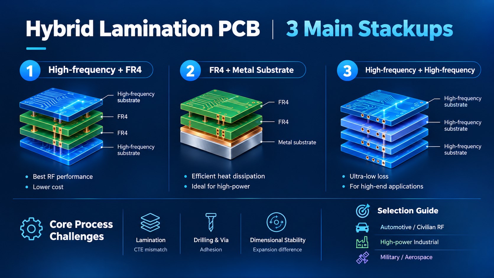
1. High-Frequency Specialty Materials + FR-4: The Top Choice for Cost-Effective RF Scenarios
Classic Combinations
Hybrid lamination of high-frequency/high-speed substrates such as Rogers RO4350B/RO4003C, PTFE, Megtron6, and Panasonic R-series with conventional FR-4.
Core Value
Zoned design is adopted: RF signal layers use high-frequency substrates, leveraging their low Dk and low Df characteristics to reduce high-frequency transmission loss, phase shift, and signal crosstalk, ensuring transmission stability; control and power layers use FR-4, relying on its mature process, good mechanical properties, and low cost to achieve the optimal balance between high-frequency performance and mass-production cost. This is the mainstream solution for RF + digital mixed circuits.
Solution Limitations
Stress differences exist at dissimilar material interfaces, and high-frequency signals crossing zones are prone to impedance discontinuity, placing higher demands on PCB layout DFM standardization. Issues such as high-frequency traces crossing zones and unreasonable zone boundaries must be avoided.
2. FR-4 + Metal Substrate: Dedicated Heat Dissipation Solution for High-Power Devices
Classic Combinations
FR-4 + aluminum substrate: strong versatility and moderate cost, suitable for conventional high-power devices; FR-4 + copper substrate: better thermal conductivity, suitable for ultra-high-power, high-heat-flux scenarios.
Core Value
It combines the advantages of high-density wiring and efficient heat dissipation: it retains FR-4's design capabilities for multilayer wiring and high-density interconnection, meeting complex circuit layout requirements; relying on the ultra-high thermal conductivity of metal substrates, it quickly dissipates concentrated heat from devices, avoiding performance degradation and device burnout caused by local overheating, greatly improving equipment operating stability. It is suitable for products such as high-power supplies, industrial control equipment, and high-power LEDs.
Solution Limitations
Limited by the physical properties of metal substrates, board layer expandability is poor, blind and buried via processes are difficult with low yield, and it is not suitable for ultra-high-density multilayer precision interconnection designs. It is only suitable for high-power, conventional wiring scenarios.
3. High-Frequency Material + High-Frequency Material: Ultimate Performance Solution for Ultra-High-Frequency Scenarios
Classic Combinations
Hybrid lamination of high-frequency substrates with different dielectric parameters, such as RO5880 (pure PTFE) + RO4350 (hydrocarbon).
Core Value
The all-high-frequency substrate architecture completely eliminates signal loss and interference caused by ordinary substrates, achieving ultra-low-loss transmission across the full frequency band, with stable dielectric characteristics and minimal temperature drift. It can meet ultra-high-frequency, ultra-high-precision transmission requirements such as millimeter-wave and terahertz applications, making it suitable for demanding scenarios such as satellite communications, high-end radar, and aerospace.
Solution Limitations
Material costs are high, multilayer high-frequency hybrid lamination processes are complex, mass-production yield is low, and delivery cycles are long. It is only suitable for high-value-added high-end precision equipment and cannot be mass-produced for civilian use on a large scale.
II. Core Process Points of Hybrid Lamination PCBs: Overcoming the Challenge of Dissimilar Material Property Differences
Quality hazards in hybrid lamination PCBs all originate from differences in physical properties among different substrates, such as coefficient of thermal expansion, surface activity, and hardness. Precise control of core processes is key to avoiding delamination, blistering, via failure, warpage offset, and ensuring yield and reliability.
1. Lamination Process: Eliminating Internal Stress and Strengthening Interfacial Bonding
CTE mismatch is the biggest pain point in lamination. For example, the parameters of PTFE (about 200 ppm/°C) and FR-4 (about 15 ppm/°C) differ greatly. Thermal cycling easily generates residual internal stress, causing interlayer delamination, board surface blistering, and board deformation. Long-term use can lead to reliability failures such as via ring cracks and BGA solder joint fractures.
The industry mainstream adopts vacuum lamination + stepped pressure and temperature ramping processes, controlling temperature and pressure in stages, precisely controlling resin flow to fill inner-layer voids, avoid uneven dielectric thickness and impedance anomalies, and optimize lamination parameters to improve interfacial bonding strength between dissimilar materials, reducing the risk of delamination and blistering at the source.
2. Drilling and Via Metallization: Solving Conductive Challenges in Inert Materials
At the boundary between soft and hard dissimilar materials, drilling resistance changes abruptly, making it prone to rough via walls, burrs, and substrate tearing. Dedicated drill bits must be matched and tool life strictly controlled to ensure drilling accuracy.
For chemically inert substrates such as PTFE, conventional copper deposition cannot adhere, making it prone to copper detachment and poor conduction. Through plasma activation and sodium naphthalene surface treatment processes, the surface activity of via walls is improved, ensuring tight adhesion of the chemical copper layer, stabilizing via metallization quality, and ensuring reliable through-hole conduction.
3. Dimensional Stability: Controlling Expansion and Shrinkage to Eliminate Warpage Offset
Different substrates have different thermal expansion and moisture absorption expansion/shrinkage coefficients. After lamination, inner-layer alignment offset and whole-board warpage are prone to occur, directly causing SMT placement defects and assembly failure.
Before production, accurately calculate the expansion/shrinkage coefficients of each substrate and perform graphic compensation in advance; during lamination, strictly control temperature gradients and cooling rates, slowly release internal stress, reduce deformation differences, ensure board dimensional accuracy and flatness, and meet precision placement and assembly requirements.
III. Core Application Areas
With flexible performance and cost-balancing capabilities, hybrid lamination PCBs have become core support for the iterative upgrading of high-end electronic equipment and are widely applied in four core areas on a large scale.
1. Communication RF
5G/6G base station AAUs, RF front ends, satellite communications, BeiDou navigation, and other equipment, solving the challenges of long-distance low-loss transmission and interference resistance for high-frequency signals.
2. Automotive Electronics
77GHz/24GHz automotive radar, ADAS advanced driver assistance, and V2X modules for connected vehicles, balancing high-frequency transmission performance with reliability under complex automotive operating conditions.
3. Aerospace and Military
Airborne radar, military communications, satellite payloads, and precision guidance equipment, adapting to harsh environments such as extreme temperature changes, high vibration, and high radiation, and meeting military requirements for high reliability and long service life.
4. Industrial and Medical
Medical imaging equipment, precision industrial sensors, high-power supplies, and high-power LED modules, balancing signal accuracy, heat dissipation efficiency, and long-term continuous operation stability.
IV. Selection Summary: The Dynamic Balance of Performance, Cost, and Mass Production
The core of hybrid lamination PCB selection is making trade-offs on demand and achieving dynamic balance: FR-4 is responsible for cost control and structural support; high-frequency substrates break through RF and high-speed performance; metal substrates solve the pain point of high-power heat dissipation.
Among these, PTFE + FR-4 hybrid lamination has the highest process difficulty, requiring overcoming the three major challenges of interfacial bonding, via metallization, and expansion/shrinkage warpage. Affected by special processes and yield, its cost is 20%-50% higher than pure FR-4, and delivery cycles are longer.
Actual selection needs to be comprehensively decided based on product positioning, performance indicators, budget, and delivery time: automotive and civilian RF applications preferably use high-frequency + FR-4 solutions; high-power industrial equipment is suitable for FR-4 + metal substrate solutions; military/aerospace and ultra-high-frequency precision equipment use all-high-frequency hybrid lamination solutions.
Standardizing DFM design in advance and precisely matching the hybrid lamination architecture can effectively avoid process risks, control production costs, achieve a win-win situation for product technical performance and commercial benefits, and provide core support for the precise implementation and stable mass production of high-end PCBs.
trending news
Contact Us