





Sorry, no sales person is available right now to take your call. Pls leave a message and we will reply to you via email as soon as possible.
How to Design RF PCBs for Low Loss and High Stability? A Complete Optimization Design Guide
2026-09-17
Overview
RF circuits are widely used in various electronic products such as communications, medical care, and industrial control. In a broad sense, the RF frequency range is 300 kHz to 300 GHz, and frequencies above 300 MHz are generally classified as the microwave range. RF signals are high-frequency analog signals, with voltage and current changing continuously over time, unlike discrete-level digital signals. RF signals rely on high-frequency carrier transmission and offer flexible bandwidth. Therefore, RF PCB design is clearly different from ordinary digital, analog, and high-speed digital PCB design. It requires special focus on high-frequency effects such as impedance control, signal loss, and electromagnetic coupling, and it is also a core challenge in many hardware engineers' designs.
Core Challenges in RF PCB Design
RF signals are highly sensitive to the electromagnetic environment. During the PCB design stage, problems such as noise interference, impedance mismatch, high signal loss, and excessive crosstalk are very likely to occur. There are four main core difficulties:
1. High Noise Sensitivity
RF circuits are highly susceptible to external noise interference and are prone to ringing and signal reflection. Improper layout and routing will directly degrade RF link transmission performance, leading to signal distortion and unstable transmission.
2. Strict Impedance Matching Requirements
Impedance matching is the core of RF design. The higher the operating frequency, the smaller the allowable impedance deviation, and the margin for error is extremely low. A common engineering rule of thumb: when trace length exceeds 1/16 of the signal wavelength, precise impedance control must be implemented (1/16 wavelength is a common industry threshold, not an absolute hard standard, and can be fine-tuned according to project specifications). For example: for a 1 GHz signal, when trace length exceeds about 375 mil, the characteristic impedance of the transmission line must be strictly controlled to avoid mismatch loss.
3. Difficult to Minimize Return Loss
In the microwave frequency range, signal return current must follow the path with minimum inductance. If the PCB ground plane is incomplete or the layout is cluttered, return current may leak into the power plane, adjacent signal layers, or nearby traces, directly causing impedance distortion, greatly increasing return loss, and weakening RF signal transmission efficiency.
4. Significant High-Frequency Crosstalk
Crosstalk intensifies as signal edge rates increase, and electromagnetic energy from the main RF trace can couple into adjacent lines. As PCB integration continues to increase and trace spacing continues to shrink, signal interference and performance degradation caused by high-frequency crosstalk will become more prominent.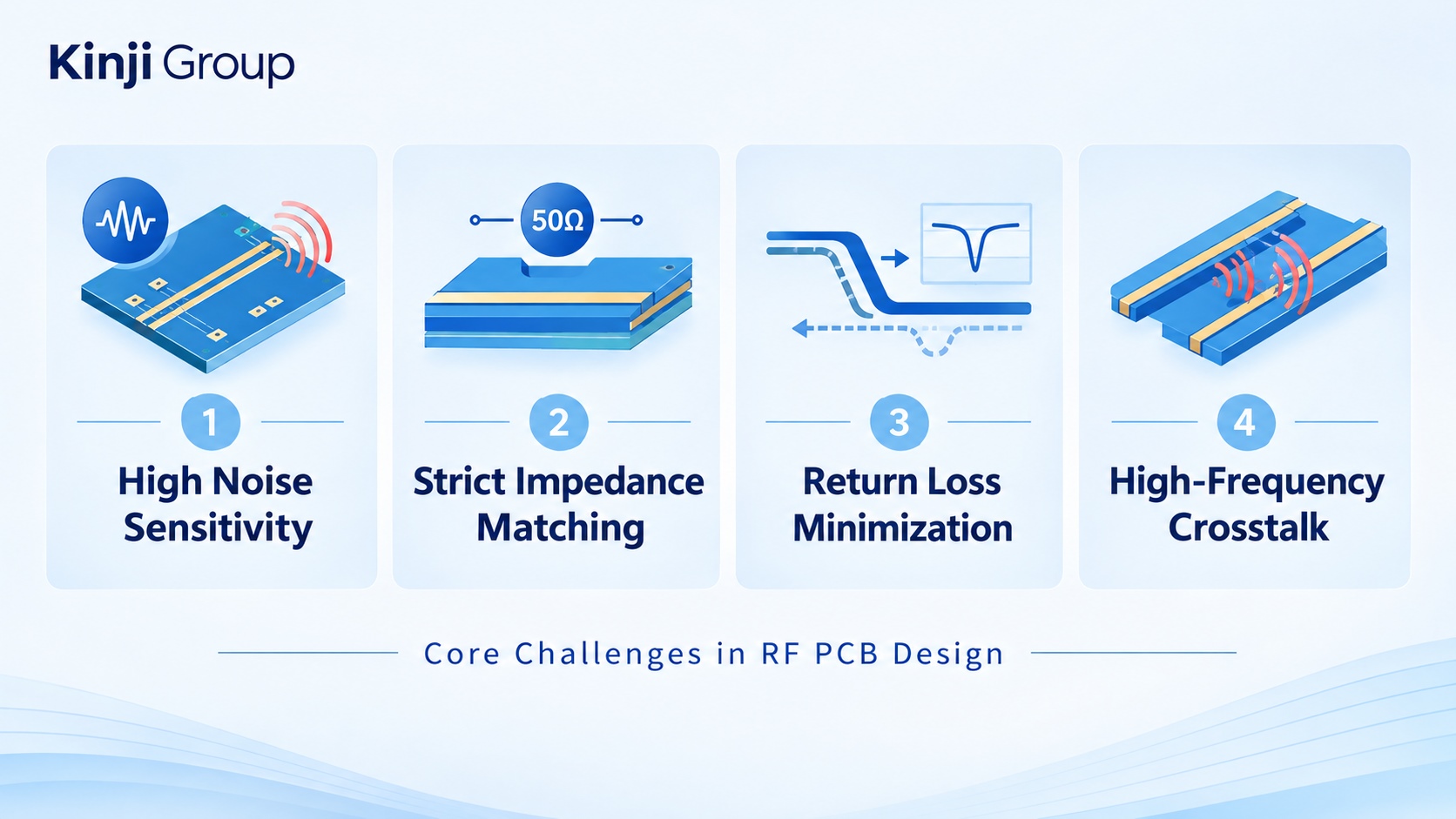
Core RF PCB Design Solutions
Noise Control Solution
Use appropriate termination schemes to precisely suppress signal reflection and ringing interference; use a complete, continuous ground plane throughout to provide a low-impedance path for signal return, fundamentally reducing noise coupling and improving circuit immunity to interference.
Precise Impedance Matching Solution
The vast majority of RF systems in the industry uniformly adopt a 50Ω standard characteristic impedance. From the signal transmitting end, to the transmission line, to the receiving end, the entire RF link must maintain continuous 50Ω impedance without abrupt changes, ensuring efficient RF energy transmission and minimizing signal reflection and energy loss.
Return Loss Optimization Solution
A complete, unbroken reference ground plane must be maintained directly beneath RF signal lines to provide a stable, low-resistance path for signal return. This design can both reduce ground loop current, eliminate stray interference, and effectively reduce leakage of RF energy to surrounding components, strictly controlling return loss.
Crosstalk Suppression Solution
· Reserve sufficient safety spacing for high-speed and sensitive RF traces, and avoid close parallel routing;
· Shorten the input and output leads of RF modules as much as possible, and keep them away from other high-speed signal lines and interference sources throughout;
· Eliminate long-distance parallel routing and greatly shorten the length of parallel coupling sections;
· In high-frequency scenarios, coplanar waveguide structures may be used, or the dielectric thickness between traces and the reference plane may be appropriately reduced to optimize transmission characteristics;
· Add ground shielding lines or a complete ground plane between adjacent signal lines, which can directly reduce high-frequency crosstalk by more than 50%.
Precise Control of RF Signal Loss
RF transmission loss is a key factor affecting high-frequency circuit performance. It is mainly divided into skin effect loss and dielectric loss, and must be controlled through both material selection and routing.
1. Skin Effect Loss
As operating frequency increases, current concentrates on the conductor surface, reducing the effective conductive cross-sectional area and greatly increasing equivalent resistance, thereby causing signal loss. In the GHz microwave frequency range, this loss intensifies sharply, directly affecting transmission distance and signal strength.
2. Dielectric Loss
When high-frequency electromagnetic waves pass through PCB dielectric material, dielectric polarization relaxation converts part of the electromagnetic energy into heat, causing energy loss. Ordinary FR4 material has a relatively high dissipation factor Df (about 0.02), and insertion loss is very obvious in high-frequency and microwave scenarios; specialized high-frequency materials such as polytetrafluoroethylene (PTFE) can have a Df as low as 0.001, greatly reducing dielectric loss and making them suitable for high-frequency precision RF circuits.
Engineering Practice Supplement: At present, mainstream products such as 5G communications and industrial RF generally adopt a high-frequency material + FR4 hybrid lamination structure, which both meets low-loss RF performance requirements and effectively controls production cost, making it the most cost-effective mass-production solution. As a professional manufacturer of high-end high-frequency and high-speed PCBs, Kinji Group has deeply cultivated hybrid lamination processes for RF high-frequency materials for many years and can stably achieve precise hybrid lamination mass production of high-frequency substrates such as Rogers RO4350B, RO4835, and 5880 with FR4. This effectively solves industry pain points such as high-frequency circuit signal attenuation, impedance shift, and excessive crosstalk. The finished products combine ultra-low transmission loss and high structural stability, and are widely suitable for high-end scenarios such as 5G base stations, automotive radar, and industrial precision RF equipment.
Key Points for RF PCB Laminate Selection
Material parameters directly determine the upper performance limit of RF PCBs. Selection should not focus only on cost. Three core indicators must be considered, adapted to different frequency-band scenarios:
1. Dissipation Factor Df
The larger the Df value, the higher the dielectric heating and signal loss at high frequencies. Ordinary FR4 has a relatively high Df and is only suitable for low-frequency RF circuits; for high-frequency and microwave scenarios above 1 GHz, low-Df specialized high-frequency materials must be selected.
2. Dielectric Constant Dk and Its Stability
The Dk value of ordinary FR4 is highly susceptible to frequency, temperature, and production batch, with fluctuations up to 10%, making it impossible to ensure impedance consistency and prone to batch performance deviation. Industrial-grade high-frequency materials such as Rogers and Nelco have extremely strong Dk parameter stability and are suitable for mass-production requirements of high-precision RF circuits.
3. Trade-off Between Dk Value and Circuit Size
In the microwave frequency range, high-Dk materials can reduce circuit footprint and support miniaturized product design, but they sacrifice bandwidth and increase loss. During selection, a precise trade-off must be made among product size, transmission bandwidth, and signal loss.
Reference for Mainstream High-Frequency Material Scenario Adaptation:
· Rogers 5880: Extremely low Df loss, mainly for millimeter-wave and high-precision low-loss microwave circuits;
· Rogers RO4350B: Balanced and stable overall performance, a general choice for 5G communication RF modules;
· Rogers RO4835: Suitable for FR4 hybrid lamination processes, balancing RF performance and production cost, suitable for mass-production projects.
RF PCB Layout and Routing | Practical Optimization Techniques
The details of layout and routing directly determine the stability and interference immunity of RF circuits. Practical design must strictly follow the following engineering guidelines:
· Plan inner layers as complete power and ground planes, using the plane structure to achieve electromagnetic shielding and minimize stray inductance interference;
· Keep the main RF signal traces as short as possible, eliminate unnecessary trace crossings and parallel coupling, and reduce signal loss;
· Prefer 45° angles or arc corners for trace turns, avoiding impedance abrupt changes and electromagnetic radiation leakage caused by right-angle turns;
· Strictly follow the principle of "routing should be short rather than long, and vias should be few rather than many" to reduce signal disturbance caused by parasitic capacitance and parasitic inductance;
· Arrange traces on adjacent signal layers orthogonally (one layer horizontal, one layer vertical) to thoroughly weaken interlayer electromagnetic coupling;
· Cover unused PCB areas fully with grounding copper foil and densely place grounding vias to build a continuous, complete shielding and grounding system;
· For critical RF links and high-frequency interference devices, metal shielding covers may be added to achieve physical spatial electromagnetic isolation;
· Prefer point-to-point topology for the main RF path, eliminate large-area signal loops, and use daisy-chain layout with caution (daisy chain is only suitable for digital control signals and is not compatible with the main RF link);
· Place decoupling capacitors close to IC power pins, extremely shortening the capacitor grounding path and efficiently suppressing power noise.
RF PCB Manufacturing Process | Key Pitfall Avoidance Points
High-quality RF design must be matched with reasonable production processes. Drawing without considering manufacturing can easily lead to the problem of perfect design but failed mass production:
· High-frequency materials have processing tolerances in Dk parameters and dielectric thickness, so process margins must be reserved during impedance design to avoid batch deviation;
· RF PCBs should preferably use ENIG surface treatment, which offers high flatness and stable impedance, is far superior to HASL, and can effectively reduce high-frequency signal loss;
· The parasitic effects of vias in high-frequency boards are prominent. In millimeter-wave and high-speed microwave scenarios, back drilling is required to eliminate via stubs and reduce signal interference;
· The processing difficulty and cost of high-frequency substrates are higher than those of ordinary FR4 boards. In the early stage of design, it is necessary to balance performance and cost according to product positioning.
Complete Closed-Loop Process for RF PCB Design
Professional RF PCB design is not completed by a single routing pass. It requires a complete closed-loop iteration to ensure performance compliance and mass producibility. Kinji Group provides a one-stop RF PCB solution covering the entire chain of design, simulation, material selection, mass production, and testing, helping projects achieve efficient implementation and finalization:
Requirement specification review → Material selection evaluation → Electromagnetic simulation (impedance, S-parameters) → Layout and routing optimization → Production file output and board release → S-parameter measurement verification → Iterative tuning and finalization.
trending news
Contact Us