





Sorry, no sales person is available right now to take your call. Pls leave a message and we will reply to you via email as soon as possible.
HDI High-Density Interconnect – Every Layer Interconnect (ELIC) Technology Explained
2026-07-13
ELIC (Every Layer Interconnect) is a core advanced process in high-end HDI (High-Density Interconnect) PCB manufacturing. Unlike traditional HDI, which relies on fixed step counts and restricted layer-to-layer interconnection, ELIC technology completely eliminates inner-layer mechanical through-holes and mechanical buried vias. Instead, it uses full laser micro-vias to achieve direct interconnection between any two layers of the circuit board, breaking the layer barriers of traditional 1-step, 2-step, and 3-step HDI. As a key technology for ultra-high-density routing and high-speed, high-frequency signal transmission scenarios, ELIC is now widely used in high-end precision electronics.
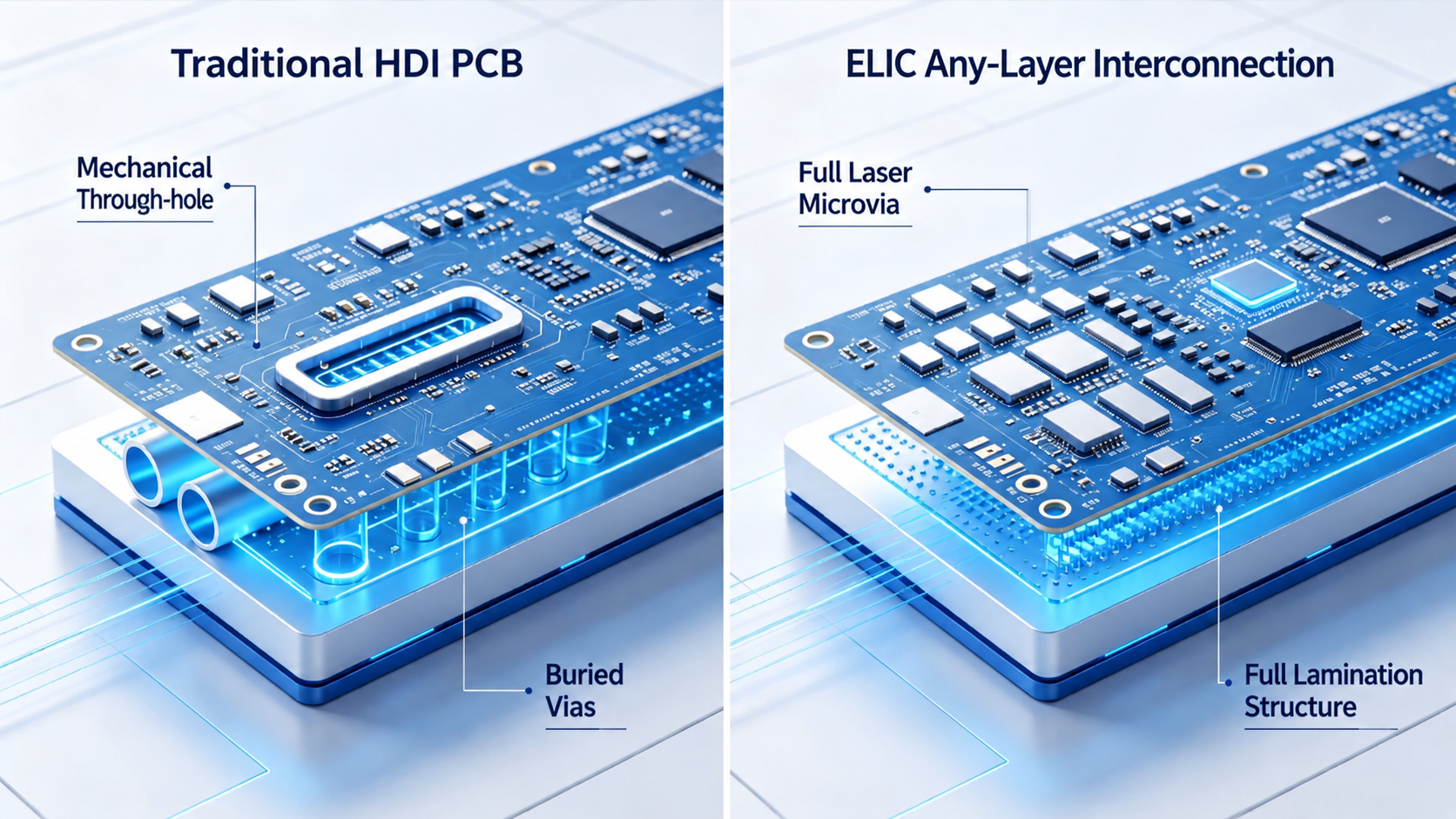

I. Core Differences Between Traditional HDI and ELIC
Traditional step-type HDI is constrained by a "core board + fixed build-up layer" structure, resulting in clear layer restrictions for interconnections and limited routing flexibility and density. In contrast, ELIC uses a fully built-up architecture, enabling unrestricted layer-to-layer conduction. The core differences are summarized in the table below:
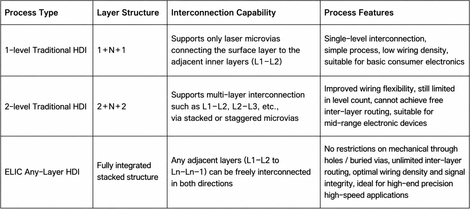

II. Core Technical Features of ELIC
ELIC achieves comprehensive upgrades across multiple dimensions including stack-up design, material systems, micro-via technology, and routing strategies, forming a high-density, high-speed, and high-reliability technical system.
1. Barrier-Free, Fully Built-Up Layer Stack-Up Design
ELIC abandons the passive step-count design of traditional "fixed core + external build-up layers" and adopts a fully built-up process involving sequential lamination, laser drilling, and layer formation. Taking a 10-layer ELIC board as an example, all adjacent layers (L1 to L10) are interconnected using high-precision laser micro-vias. There is no core board structure constraint and no layer-to-layer conduction barriers. The stack-up can be flexibly planned according to product requirements, meeting the demands of high-layer-count, high-precision routing.
2. Low-Loss, Ultra-Thin, High-End Material System
To match ultra-high-density routing and high-speed, high-frequency signal transmission, ELIC utilizes low-loss, ultra-thin substrates and auxiliary materials, reducing signal loss from the source and improving routing precision:
o Dielectric Layers: Utilize 50–100μm ultra-thin prepreg (PP) materials, combined with high-end substrates featuring low Dk (Dielectric Constant) and low dissipation factor, effectively reducing dielectric loss and delay in high-frequency signal transmission, thus ensuring signal integrity.
o Conductive Layers: Employ 12–18μm ultra-thin copper foil (1/3 oz to 1/2 oz), supporting ultra-fine circuit processing and meeting mass production requirements for ≤50μm line width/spacing.
3. High-Precision Laser Micro-Via Process Specifications
All interlayer connection vias in ELIC are formed using UV/CO₂ laser drilling. Compared to traditional mechanical drilling, this results in smaller via diameters, higher precision, and significantly improved space utilization. Key process parameters include:
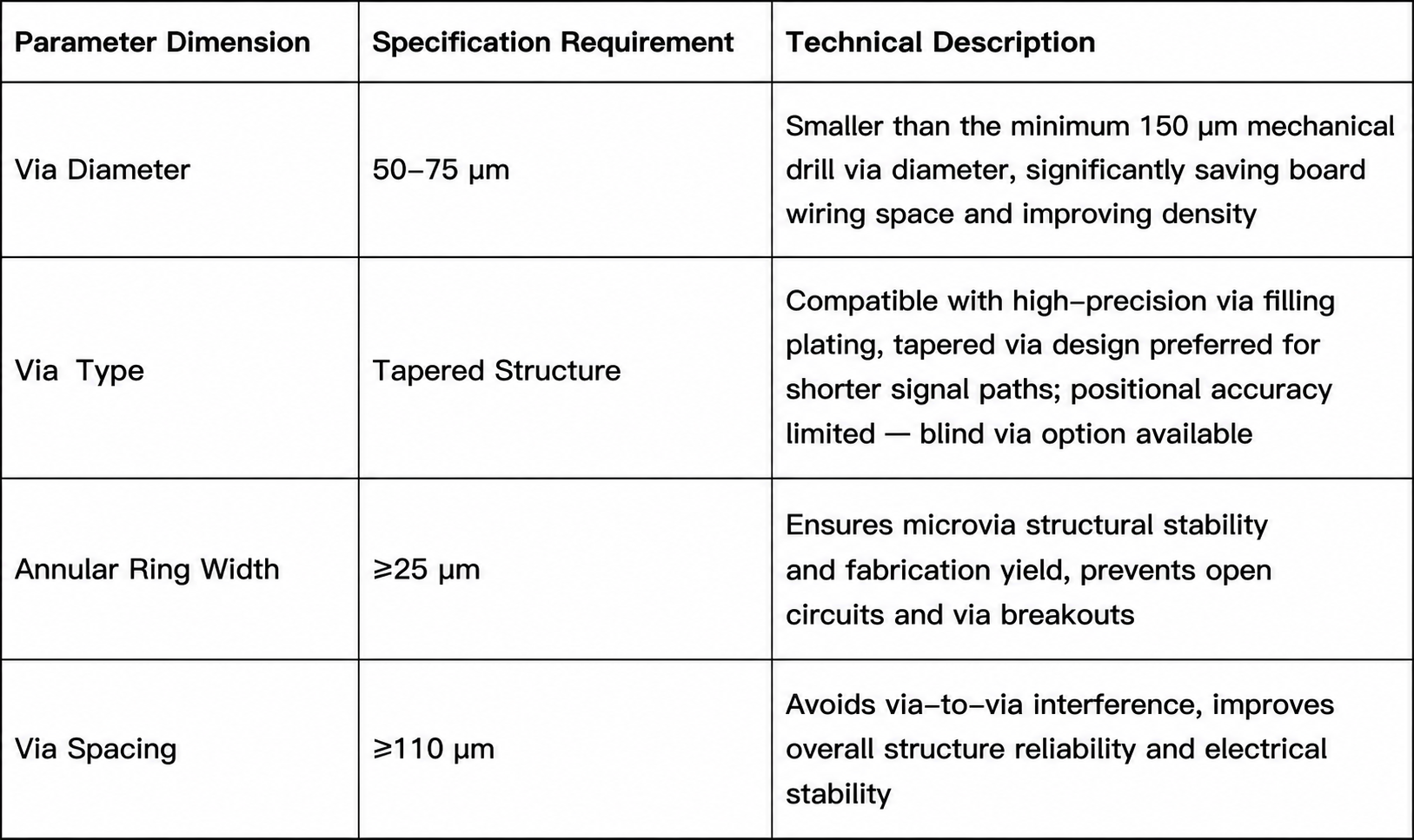

4. High-Density Routing and BGA Optimized Fan-Out Strategy
By completely eliminating inner-layer mechanical buried vias, ELIC frees up significant inner-layer routing area, making it ideally suited for ultra-high-precision package devices like 0.3mm fine-pitch BGAs. Device pads can be directly connected vertically via "one-to-one" laser micro-vias to the next layer, eliminating the need for surface routing or extra transition vias, thereby removing surface trace interference at the source.
Furthermore, the any-layer direct connection architecture completely eliminates the stub effect inherent in traditional through-holes, significantly reducing loss, crosstalk, and reflection in high-speed signal transmission, and optimally enhancing signal integrity in high-frequency, high-speed scenarios.
5. Standardized Stack-Up and Electrical Network Planning
ELIC employs an "all-PP dielectric + ultra-thin copper foil" integrated core-less stack-up structure. A typical stack-up arrangement is: L1 (Signal) - PP Dielectric - L2 (Signal/Power) - PP Dielectric - ... - Ln (Signal), allowing for flexible and unconstrained layer combinations.
Electrical network planning follows high-speed, stable principles: Power and ground networks are concentrated on inner layers to ensure stable power supply and good grounding for the entire system; high-speed signal lines are preferentially routed on outer and near-outer layers; interlayer signal transitions strictly follow the shortest path principle to minimize signal attenuation and delay.
6. Ultra-Fine Routing Parameter Standards
Leveraging precision materials and laser micromachining technology, ELIC achieves ultra-high-precision circuit fabrication. Key mass production parameters include: Minimum line width/spacing of 40/40μm, and line impedance tolerance controlled within ±10%, meeting the impedance matching requirements of high-end precision circuits.
III. ELIC Process Flow and Quality Control Standards
1. Core Process Flow
ELIC utilizes a closed-loop, sequential layer-by-layer build-up process. The standardized process flow is: Single-layer lamination → Precision laser micro-via drilling → Plating via filling and curing. This bidirectional, layer-by-layer process completes the entire board build-up. Closed-loop control throughout the process ensures consistency in lamination precision, drilling quality, and plating quality for each layer, guaranteeing the stability and uniformity of interconnections across all levels.
2. Layer-to-Layer Alignment Precision Standards
High-precision alignment is a fundamental requirement for the ELIC process. Stringent mass production standards mandate: Overall board layer-to-layer alignment deviation ≤ ±25μm, and stacked via vertical offset ≤ 15μm, effectively preventing process defects such as layer misregistration, via misalignment, and short circuits.
3. Laser Micro-Via Filling Quality Standards
All laser micro-vias must achieve 100% complete copper plating fill. The via surface must be smooth and flat, free from visual defects like dimples, protrusions, or pinholes. The via interior must be free of voids, gaps, or contaminants to prevent potential failures such as oxidation, open circuits, or abnormal resistance during long-term use, ensuring the long-term reliability of the circuit board.
4. Key DFM Pre-Verification Points
A comprehensive Design for Manufacturability (DFM) check is required before mass production. Key focus areas include verifying layer-to-layer alignment deviation, plating fill quality, micro-via annular ring width, via-to-via spacing, line width/spacing, impedance parameters, etc. This proactively resolves design-process conflicts, stabilizes production yield, and ensures the product's electrical performance and structural reliability.
IV. Application Scenarios and Cost Characteristics
1. Primary Application Scenarios
Leveraging its ultra-high wiring density, superior high-speed signal integrity, and excellent structural reliability, ELIC is primarily suited for high-end precision, high-speed/high-frequency, and miniaturized electronic devices. Typical applications include:
o Motherboards for flagship smartphones and foldable phones
o Precision packaging substrates for high-end CPUs and GPUs
o High-frequency PCBs for 5G/6G communication base stations
o High-speed server and cloud computing mainboards
o High-frequency communication PCBs for military radar and aerospace applications
2. Cost Characteristics
The overall cost of ELIC is relatively high, primarily due to the high cost of ultra-thin, high-end substrates, significant investment in precision laser micro-via processing equipment, the complex sequential build-up process, and extremely stringent process control requirements. For the same layer count, the cost of an ELIC any-layer interconnect PCB is more than double that of a standard high-end step-type HDI. This cost premium increases with layer count and process complexity, positioning ELIC as a classic "high-performance, high-cost" high-end PCB technology.
V. Comprehensive Comparison of Mainstream HDI Technologies
To clearly differentiate the application scenarios and performance capabilities of various HDI process levels, a comparison of 1-step HDI, 2-step HDI, and ELIC is provided below across multiple dimensions including structure, interconnection capability, performance, and cost:
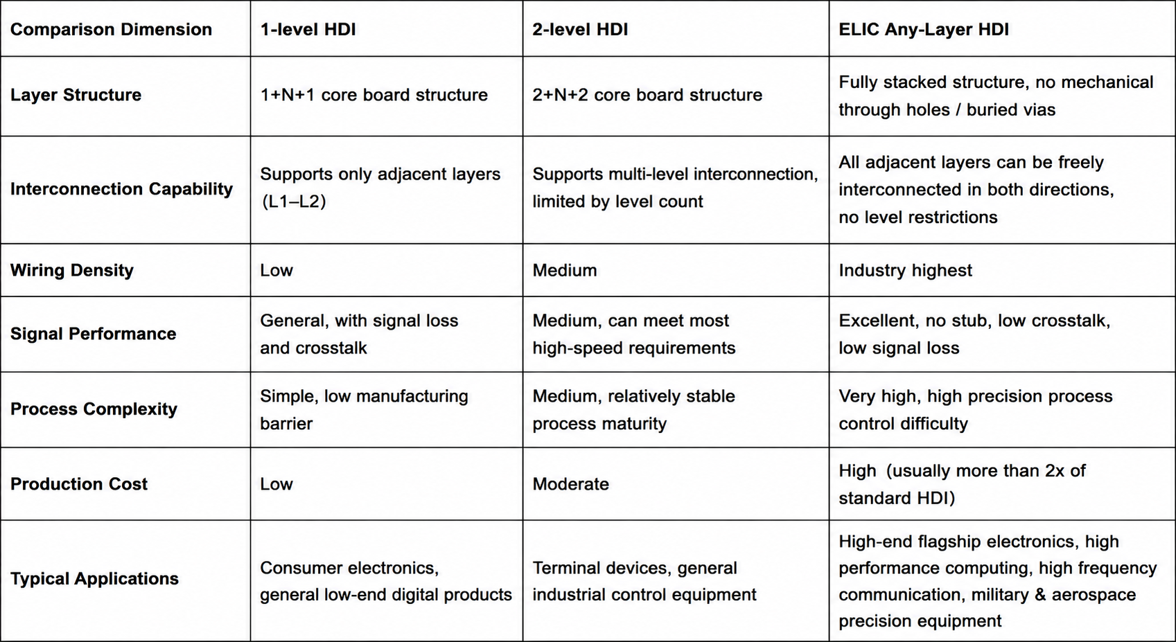
ELIC (Every Layer Interconnect) technology breaks through the structural and process bottlenecks of traditional step-type HDI. Through its innovative architecture featuring full laser micro-vias, elimination of mechanical vias, and a fully built-up construction, it achieves maximum freedom in PCB layer-to-layer interconnection and the highest routing density. Simultaneously, it fundamentally optimizes high-speed signal transmission performance, making it perfectly suited for the high-density, high-speed, and high-reliability interconnection needs of cutting-edge fields like 5G high-frequency communications, AI smart hardware, high-end computing, and precision packaging. However, due to its complex process and high cost, careful selection based on performance requirements and budget constraints is necessary during product design and mass production to achieve an optimal balance between performance and cost.
trending news
Contact Us