





Sorry, no sales person is available right now to take your call. Pls leave a message and we will reply to you via email as soon as possible.
Guide to Charging Pile PCB Prototyping Selection and High-Temperature/High-Voltage Process Matching
2026-09-14
I. Analysis of Harsh Operating Conditions: Why Conventional PCB Solutions Cannot Adapt to Charging Piles
Charging pile PCBs operate long-term in a complex coupled field of high voltage, high current, high temperature rise, and harsh outdoor environments. If conventional consumer electronics or ordinary industrial board solutions are directly used (such as standard 1oz copper thickness and Low-Tg FR-4), serious failure modes such as delamination, insulation breakdown, thermal runaway board burning, and electrochemical migration (ECM) are highly likely to occur due to lack of thermal stability, insufficient insulation margin, and poor anti-corrosion performance.

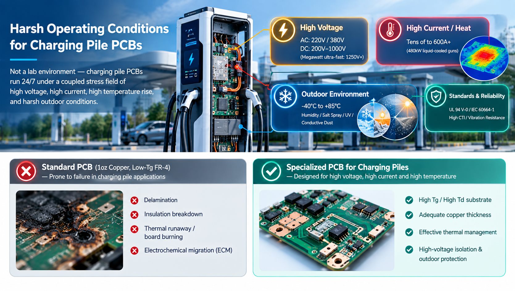
Typical engineering operating conditions and performance benchmarks:
· High-voltage strong-current architecture: AC piles 220V/380V; DC fast-charging piles 200V–1000V (the operating voltage of megawatt-level heavy truck ultra-fast charging systems can reach 1250V and above).
· High current and transient temperature rise: Operating current covers tens to hundreds of amperes (for example, the peak current of a 480kW liquid-cooled ultra-fast charging gun cable reaches 600A+), and the local power density of power devices (SiC/IGBT) is extremely high, with severe transient temperature rise.
· All-weather outdoor stress: Must meet -40°C~+85°C wide-temperature operation and withstand long-term high humidity, salt spray, ultraviolet radiation, and conductive dust deposition.
· High-standard compliance: Must strictly comply with industry mandatory standards such as UL 94 V-0 flame retardancy, IEC 60664-1 insulation protection, high CTI tracking resistance, and vibration resistance.
II. Accurate Substrate Selection: The Physical Cornerstone of High Temperature Resistance and High Voltage Resistance
The physical and electrical properties of PCB substrates determine the temperature resistance limit, insulation grade, current-carrying capacity, and heat dissipation efficiency of the circuit board. Engineering selection must focus on checking Tg (glass transition temperature), Td (decomposition temperature), CTI (comparative tracking index), and copper foil thickness.
1. Tg / Td / CTI Values: Defining the Limit Performance of Substrates
Tg (glass transition temperature): Controls the mechanical rigidity and dimensional stability of the substrate at high temperatures. Engineering criterion: measured maximum board surface temperature + 20°C ≤ Tg.
Td (decomposition temperature): Requires Td≥340∘CTd≥340∘C (5% weight loss temperature) to ensure that resin decomposition or interlayer delamination does not occur during lead-free soldering and multiple reworks.
CTI (comparative tracking index): Substrates in high-voltage areas must reach CTI ≥ 600V (PLC level 0), greatly reducing the required creepage distance.

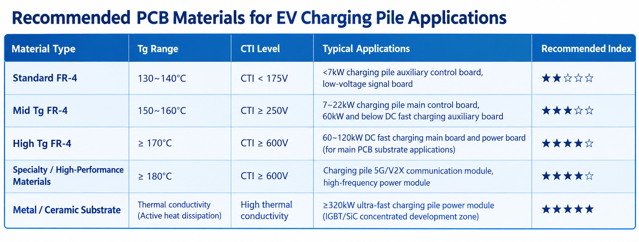
Note: In actual R&D prototyping, Kinji Group's supply chain system has fully covered from high-Tg FR-4 to aluminum nitride ceramic substrates, copper substrates, and heterogeneous laminated materials, and can support rapid prototyping and customization for multiple power gradients.
2. Copper Foil Thickness: Matching Current-Carrying Capacity and Thermal Management
Copper thickness selection directly determines line impedance, conductor temperature rise, and thermal loss:
· Signal and low-voltage control layers: Use 1oz (35um) standard copper thickness to ensure fine wiring density.
· Power and main power loop: Use 2~4oz (70~140um) thickened copper foil.
· Extremely high-current main channels: Use local 70~400um ultra-thick copper or embedded copper block (Embedded Copper) processes.
III. Four Core Process Combinations for High Temperature Resistance and High Voltage Resistance
For high-voltage and high-current operating conditions, systematic process control must be implemented on the manufacturing side:
1. Solder Mask and Surface Treatment Processes
Thickened solder mask: Use high-insulation, high-heat-resistant solder mask ink, and perform secondary printing or thickened coating on high-voltage and large copper areas (ink thickness ≥ 25um) to prevent ink carbonization, cracking, or peeling under long-term high-temperature operation.
Surface treatment: Outdoor core power boards preferably use Electroless Nickel Electroless Palladium Immersion Gold (ENEPIG) or thickened Immersion Gold (ENIG) to ensure excellent salt spray resistance, corrosion resistance, and multiple reflow soldering reliability; low-voltage control boards may use lead-free hot air solder leveling (HASL).
2. High-Voltage Insulation and Breakdown Resistance Processes
Creepage distance and electrical clearance: Designed according to IEC 60664-1 pollution degree 3 standards. For a 1000V DC system, the high-low voltage isolation band must maintain ≥8.0mm (a 10mm margin is recommended), combined with board-edge routing slots to block surface leakage paths.
Inner-layer dielectric thickness: The total thickness design of prepreg (PP) between high-voltage layers of multilayer power boards must meet insulation withstand voltage requirements (usually ≥0.2mm/200um) to prevent dielectric breakdown.
3. Thermal Management and Efficient Heat Dissipation Processes
Thermal via arrays: Densely arrange copper-plated thermal vias under power device (MOSFET, diode) pads (recommended aperture 0.3~0.5mm, via wall copper thickness ≥20um), and use via plugging and solder mask covering/resin filling and plating flat (POHV/VIPPO) processes to balance thermal conduction and soldering flatness.
Lamination and metal base bonding: Use a laminated structure of FR-4 with aluminum/copper substrates to quickly conduct heat from the power loop to the base heat sink.
4. Outdoor Environment Protection Processes
Automated conformal coating spraying: After PCB assembly, apply acrylic or silicone conformal coating (protective film thickness 30~60um) to prevent moisture, salt spray, and mold.
Vibration reinforcement: Add teardrop designs to heavy components and high-voltage connector pads, and perform mechanical locking or dispensing reinforcement to withstand low-frequency vibration during long-term operation.
IV. Practical Prototyping Selection Solutions for Different Scenarios

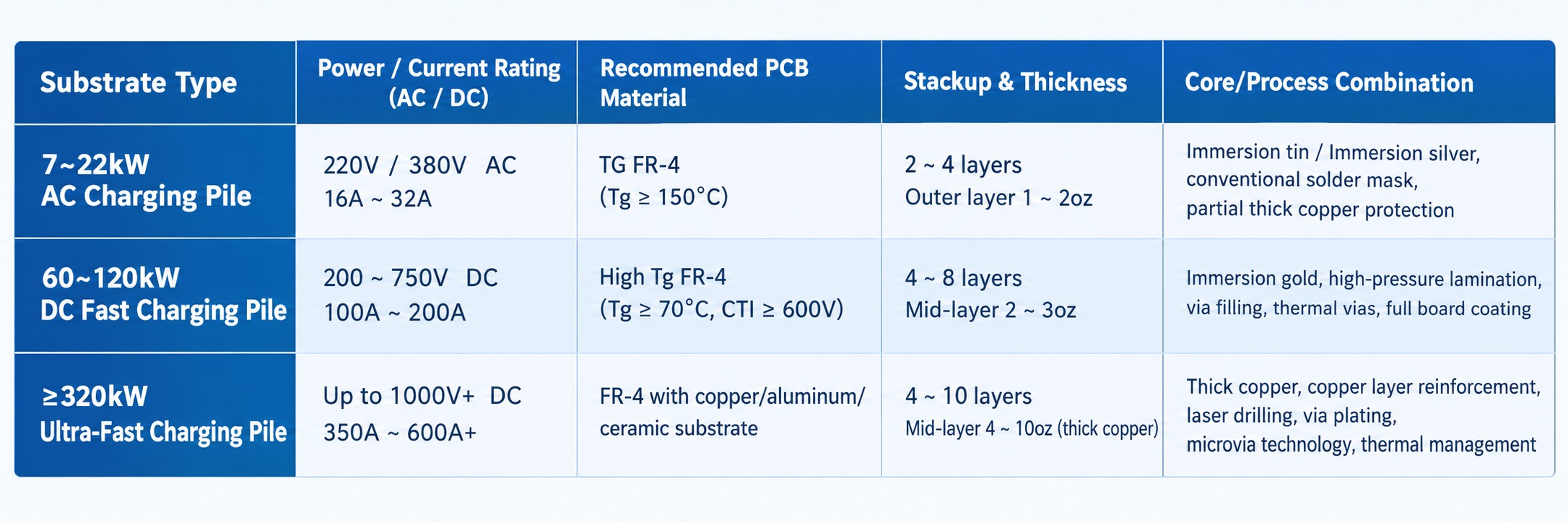
In specific project implementation, Kinji Group's automated CAM analysis system can automatically match the above process parameters based on Gerber files and provide a "DFM Manufacturability and Reliability Assessment Report" before production, eliminating potential revision risks at the drawing stage.
V. FAQ: Analysis of High-Frequency Questions in Charging Pile PCB Design and Processes
1. Design Parameter Calculation
Q1: How to accurately select high-Tg materials? How to convert between Tg value and actual temperature rise?
Engineering criterion: Tg ≥ maximum ambient temperature + temperature rise caused by current + 20°C (safety margin).
Example: If the extreme ambient temperature inside the outdoor cabinet is 55°C and the local temperature rise in the power area reaches 95°C, then the maximum board surface temperature is 150°C. The theoretical calculated Tg value is ≥ 170, so a high-Tg170 material must be selected. At the same time, it is necessary to ensure Td ≥ 340°C and CTI ≥600V, and all three indicators must be satisfied simultaneously.
Q2: How to scientifically design the aperture, number, and spacing of thermal vias?
Aperture: 0.3mm~0.5mm is recommended. An aperture smaller than 0.3mm easily leads to uneven electroplating filling or gas entrapment in microvias; an aperture larger than 0.5mm easily causes solder loss (cold solder joints) of SMD components during wave soldering/reflow soldering.
Spacing: The center-to-center distance of vias is recommended to be maintained at 1.0mm~1.2mm. Too dense will cut the ground plane (ground island effect), while too sparse will fail to form an efficient thermal conduction channel.
Thermal resistance estimation and quantity: The thermal resistance of a single 0.3mm aperture (20um wall thickness) copper-plated via is about 15~20°C/W. For a device with 10W power consumption and allowable temperature rise of 20°C, at least 10W X 18°C/W / 20°C ≈ 9 thermal vias need to be arranged (such as a 3 x 3 array).
Q3: What are the minimum line width/spacing (W/S) limits for thick copper boards (≥3oz)?
The etching process has an undercut phenomenon, and increased copper thickness leads to greater undercut. Design margin formula:
Production design spacing ≥ theoretical limit spacing / 0.8
Conventional recommended design guidelines:
1oz (35um): Minimum line width/spacing ≥0.10/0.10 (4/4 mil)
2oz (70um): Minimum line width/spacing ≥ 0.15 / 0.15 (6/6 mil)
3oz (105um): Minimum line width/spacing ≥0.20/0.20 (8/8 mil)
Q4: How to accurately calculate high-voltage creepage distance according to IEC 60664-1?
According to pollution degree 3 (outdoor industrial environment) and material group I (CTI ≥ 600V):
Working voltage 600V DC: Minimum creepage distance is 6.3mm.
Working voltage 1000V DC: Minimum creepage distance is 10.0mm.
Altitude correction: If the equipment is installed in areas above 2000 meters altitude, multiply by the altitude correction factor (for example, multiply by 1.29 at 4000 meters). In engineering design, it is recommended to reserve an additional 15%~20% safety margin, or improve air gap insulation performance through slot isolation (slot width ≥1.0).
2. Process Defect Prevention and Control
Q5: Thick copper boards have severe etching undercut. How to coordinate prevention and control from the design side and CAM stage?
CAM deep compensation: The board manufacturer must perform reverse line width compensation in the CAM stage according to copper thickness (≈ x0.25 x copper thickness). For example, in Kinji Group's manufacturing process, the system automatically fits the undercut factor curve according to the selected copper thickness to ensure that the conductor cross-sectional area after etching meets the rated current-carrying requirements.
Design-side optimization:
Avoid right-angle and acute-angle routing, and uniformly use R≥0.5mm arcs or 135° chamfers at corners to reduce the risk of tip discharge and local over-etching.
Large-area power copper layers need to use grid copper or uniformly distributed thermal holes to facilitate uniform flow of etching solution and avoid residual copper short circuits caused by the "pond effect."
Q6: What defects are likely to occur during lamination of mixed structures (FR-4 + metal/ceramic substrates)?
Interfacial delamination: Caused by CTE (coefficient of thermal expansion) mismatch of heterogeneous materials and insufficient surface adhesion. Prevention and control: Metal/ceramic surfaces must undergo physical roughening or Plasma treatment; use high-flowability, high-adhesion Prepreg. Kinji Group is equipped with a dedicated lamination parameter database for mixed structures, ensuring bonding strength between heterogeneous dielectric layers through multi-stage temperature control and pressure gradient control.
Warpage: Uneven release of internal stress during lamination cooling. Prevention and control: Strictly implement symmetric lamination design, match copper weight distribution of each layer, and introduce a stepped slow cooling process in the CAM lamination curve.
VI. Summary
The selection and manufacturing of charging pile PCBs is a comprehensive test of electrical, thermal, and material engineering. From the selection of high-Tg, high-CTI substrates to the matching of thick copper current-carrying, high-voltage isolation, and thermal vias, every link requires close collaboration between design engineers and manufacturers.
By establishing standardized calculation models (such as IPC-2152 and IEC 60664-1) and introducing suppliers such as Kinji Group with special board manufacturing and pre-production DFM review capabilities during the prototyping stage, the sample verification cycle can be significantly shortened, failure risks in subsequent mass production can be reduced, and a new generation of high-reliability, long-life charging pile core modules can be created.
trending news
Contact Us