





Sorry, no sales person is available right now to take your call. Pls leave a message and we will reply to you via email as soon as possible.
Packaging Processes and Applications of Ceramic Substrates
2026-09-11
Ceramic substrates, also known as ceramic circuit boards, are mainly composed of a ceramic base and a surface metal circuit layer. In electronic packaging, the packaging substrate plays a key role as a bridge, connecting internal and external heat dissipation paths, and simultaneously serves important functions such as electrical interconnection, mechanical support, and heat dissipation. Because ceramic materials have characteristics such as high thermal conductivity, good heat resistance, excellent mechanical strength, and a low coefficient of thermal expansion, they have become a commonly used substrate material in power semiconductor device packaging. According to packaging structures and application requirements, ceramic substrates can mainly be divided into two major categories: planar ceramic substrates and three-dimensional ceramic substrates.
I. Planar Ceramic Substrates
According to different preparation principles and processes, planar ceramic substrates are mainly divided into the following categories:

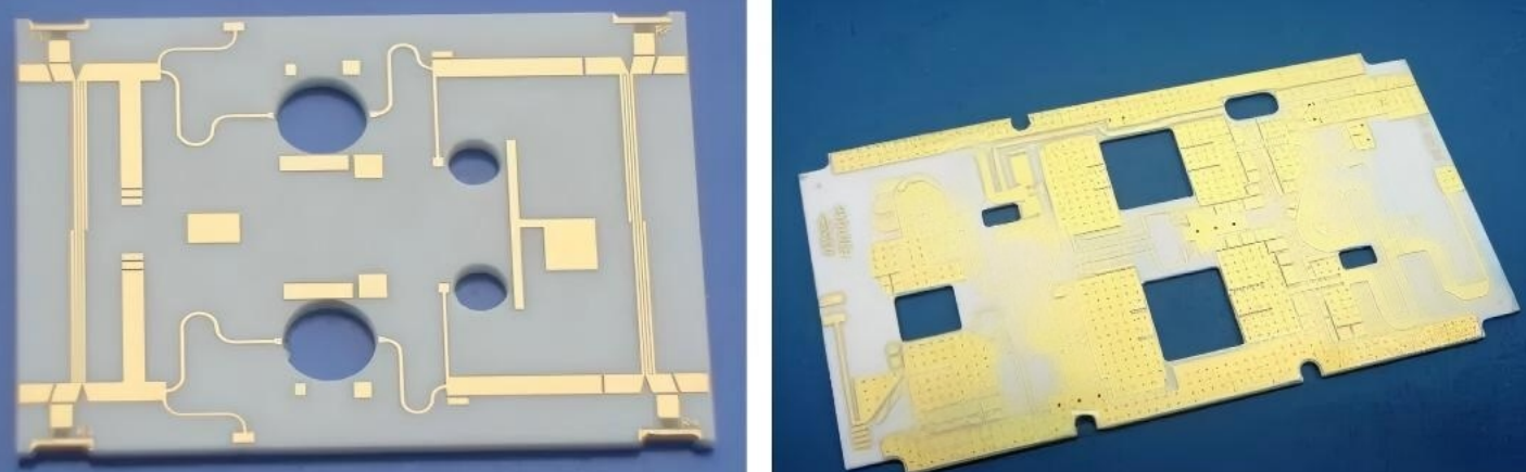
Thin-Film Ceramic Substrate (TFC) Products

TPC Substrate Preparation Process Flowchart
1. Thin-Film Ceramic Substrate (TFC)
A sputtering process is used to directly deposit a metal layer on the surface of a ceramic substrate, and the metal layer can be patterned into circuits through processes such as photolithography, development, and etching. Because the sputtering deposition rate is low (usually below 1 μm/h), the metal layer of TFC substrates is relatively thin (generally less than 1 μm), enabling high pattern precision (line width/spacing less than 10 μm). It is mainly used for packaging small-current devices in fields such as lasers and optical communications.
2. Thick-Film Printed Ceramic Substrate (TPC)
Metal paste is coated onto a ceramic substrate by screen printing, then dried and sintered at high temperature (850°C–900°C) to form circuits. The metal layer thickness is usually 10–20 μm, and the thickness can be increased through multiple printing passes. TPC substrates have a simple process and low cost, but due to the limitations of screen printing, circuit precision is relatively low (minimum line width/spacing generally greater than 100 μm), and the glass phase added to the metal paste reduces its electrical and thermal conductivity. Therefore, it is mostly used in fields such as automotive electronics that do not require high circuit precision.
The key technology of TPC substrates lies in the metal paste: the paste is generally composed of metal powder, an organic carrier, and glass powder. Silver-based conductive paste occupies the mainstream position because of its good electrical and thermal conductivity and relatively low cost. Studies have shown that the particle size, morphology, and other characteristics of silver particles have a significant impact on conductive performance. The organic carrier determines the rheological properties of the paste, affecting printing quality and densification after sintering. The addition of glass powder can lower the sintering temperature, and environmentally friendly lead-free glass powder is currently a research and development focus.
3. Direct Bonded Copper Ceramic Substrate (DBC)
Oxygen is introduced between copper foil and a ceramic substrate (such as Al₂O₃ or AlN), and at high temperature (about 1065°C), a Cu/O eutectic phase forms, which then reacts with the ceramic to form compounds, achieving eutectic bonding between the copper foil and the ceramic. DBC substrates have good thermal conductivity, high bonding strength, and excellent thermal stability. The copper foil thickness is usually 100–600 μm, making them suitable for high-current, high-temperature operating environments such as IGBTs, lasers, and concentrated photovoltaics. However, their process has strict requirements for temperature and oxygen content control, resulting in relatively high production costs, and due to the limitations of thick copper etching, it is difficult to achieve high-precision circuits.

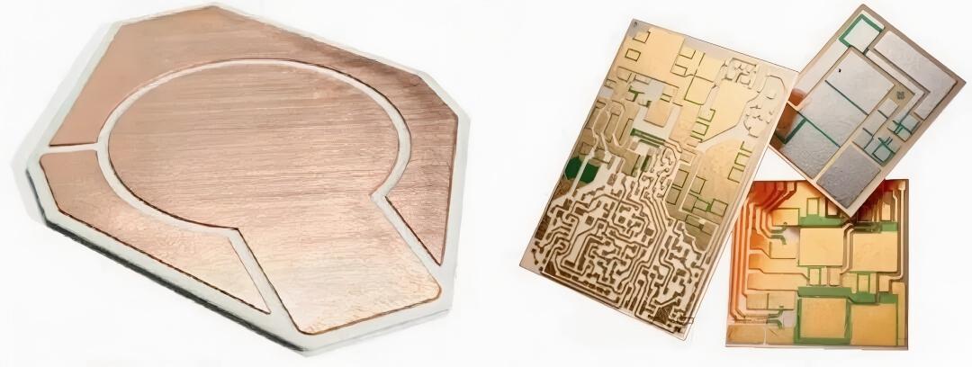
DBC Ceramic Substrate Products


DBC Ceramic Substrate Preparation Process Flow
4. Active Metal Brazing Ceramic Substrate (AMB)
An active metal braze (such as Ag-Cu-Ti) is added between the copper foil and the ceramic, and welding is achieved under vacuum at high temperature. AMB substrates have high bonding strength and good thermal cycling performance, making them especially suitable for fields such as automotive power modules with stringent reliability requirements.
5. Direct Plated Copper Ceramic Substrate (DPC)
Processes such as laser drilling, patterned masking, and electroplating are used to form copper circuits on the ceramic surface. DPC substrates have high circuit precision and can achieve vertical interconnection, making them suitable for high-density packaging. However, the metal layer thickness is limited, so they are generally suitable for small- and medium-power devices.
6. Laser Activated Metallization Ceramic Substrate (LAM)
Laser activation treatment is performed on the ceramic surface, followed by electroless plating or electroplating to form metal circuits. This process is suitable for localized metallization and fine circuit fabrication and offers good design flexibility.
II. Three-Dimensional Ceramic Substrate Preparation Technologies
Three-dimensional ceramic substrates add three-dimensional structures such as cavities and steps on the basis of planar substrates to meet more complex packaging requirements. Common types include:

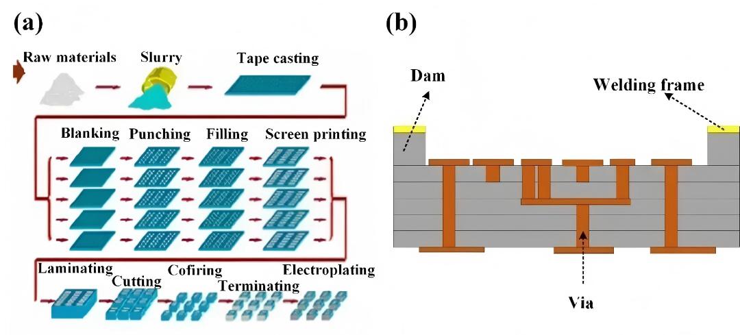
(a) HTCC Ceramic Substrate Preparation Process Flow and (b) Structural Schematic Diagram

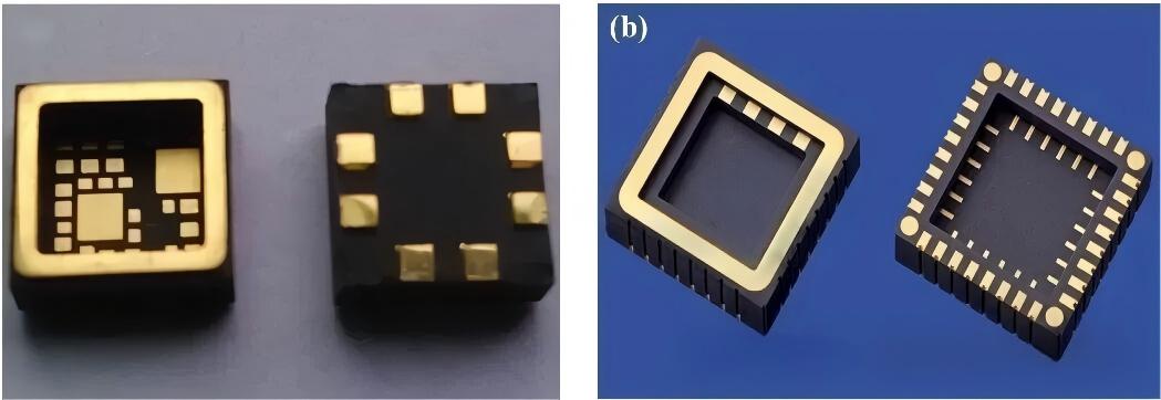
(a) HTCC Ceramic Substrate Products and (b) LTCC Ceramic Substrate Products
1. High-/Low-Temperature Co-Fired Ceramic Substrates (HTCC/LTCC)
HTCC: High-temperature sintering (about 1600°C) is used, and ceramic green bodies are co-fired with high-melting-point metal pastes such as tungsten and molybdenum. It has advantages such as high mechanical strength, good thermal conductivity, and high stability, but the metal conductivity is relatively poor and the cost is high.
LTCC: Glass powder is added to the ceramic to lower the sintering temperature (usually 850–900°C), allowing the use of metal pastes with good conductivity such as silver and copper. It has characteristics such as low process temperature, adjustable dielectric properties, and suitability for multilayer wiring, and is widely used in high-frequency, high-reliability fields such as aerospace and military electronics.

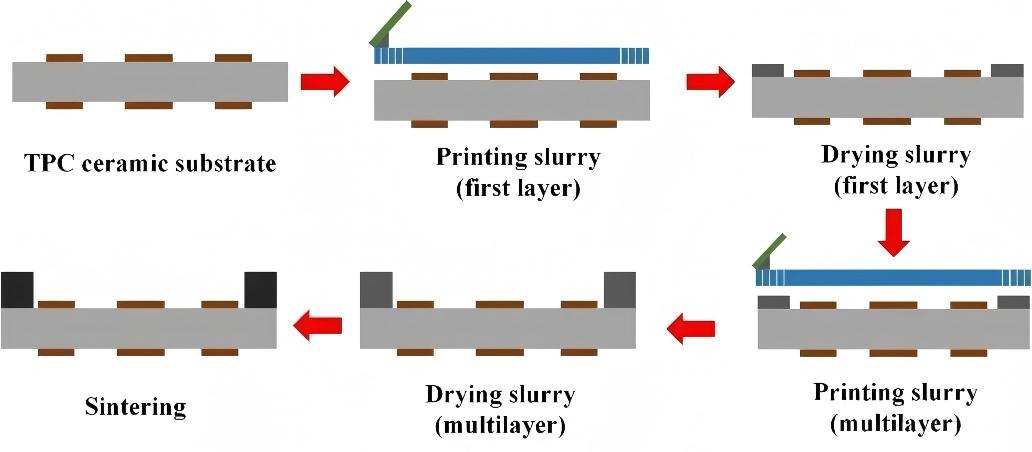
MSC Ceramic Substrate Preparation Process Flow

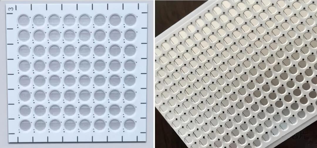
MSC Three-Dimensional Ceramic Substrate Products
2. Multilayer Sintered Three-Dimensional Ceramic Substrate (MSC)
On a planar TPC substrate, ceramic paste is screen-printed multiple times and sintered to form a cavity structure. Its advantages include a simple process and good thermal expansion matching, but due to the limitations of screen printing, cavity thickness and circuit precision are limited, making it suitable for packaging small devices that do not require high precision.

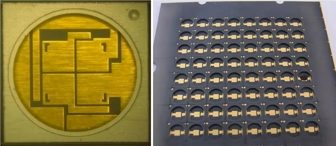
DAC Ceramic Substrate Products Prepared by Organic Adhesive Bonding

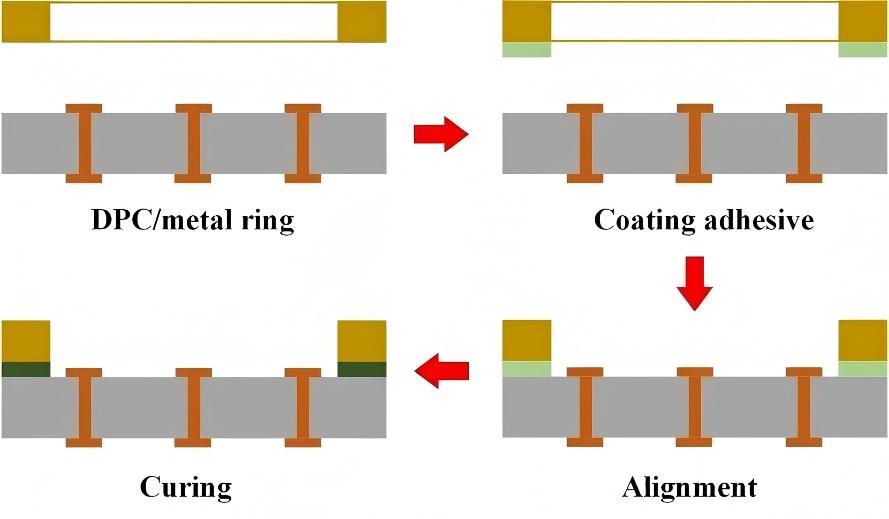
DAC Three-Dimensional Ceramic Substrate Preparation Process Flow
3. Direct Adhesive-Bonded Three-Dimensional Ceramic Substrate (DAC)
A metal or ceramic ring is bonded to a high-precision DPC substrate at low temperature using an organic adhesive. This process is simple, low in cost, and does not damage the DPC circuit layer. However, the organic adhesive has poor heat resistance and airtightness, making it suitable for packaging high-precision devices that do not have high heat dissipation and sealing requirements.
4. Multilayer Copper-Plated Three-Dimensional Ceramic Substrate (MPC)
Three-dimensional copper structures are built on a ceramic substrate through multiple patterned electroplating steps, enabling high-precision, high-thermal-conductivity three-dimensional circuits, but the process steps are relatively complex.
5. Direct Molded Three-Dimensional Ceramic Substrate (DMC)
Injection molding or die-casting is used to form a ceramic substrate with a three-dimensional structure in one step, followed by metallization treatment to form circuits. It is suitable for mass-produced products with complex structures, but mold costs are high and precision is limited by the molding process.
Summary
According to different application scenarios, ceramic substrate technologies show diversified development in material selection, process methods, and performance emphasis. Planar ceramic substrates, represented by TFC, TPC, DBC, AMB, and others, meet different needs such as high precision, low cost, and high power. Three-dimensional ceramic substrates, through processes such as HTCC/LTCC, MSC, and DAC, provide more possibilities in structural integration and functional expansion. In the future, with the development of fields such as power electronics, RF modules, and optoelectronic integration, ceramic substrates will continue to evolve toward higher thermal conductivity, higher precision, higher reliability, and better cost.
trending news
Contact Us