



Sorry, no sales person is available right now to take your call. Pls leave a message and we will reply to you via email as soon as possible.
Diamond Semiconductors: Cooling Is Commercial, Chips Are Still Years Away
2026-11-03
Diamond is an ultra-wide bandgap (UWBG) semiconductor with a bandgap of about 5.47 eV. In theory, its breakdown field strength, thermal conductivity and high-temperature tolerance all point to the performance limits of power devices, which is why it is called the "ultimate semiconductor." But any discussion of diamond's industrialization must first draw a key distinction:
Diamond substrates/heatsinks for cooling (used as a high-thermal-conductivity material that does not carry transistor functions) have already entered small-volume commercial production; diamond active devices (transistors/diodes in which diamond itself serves as the channel or drift layer) remain at the laboratory prototype stage.
These two tracks differ in maturity by at least an order of magnitude. Confusing them would seriously overestimate how quickly diamond semiconductors will land in the near term.
I. Comparison of Core Material Parameters
| Parameter | Silicon (Si) | Silicon Carbide (SiC) | Gallium Nitride (GaN) | Single-Crystal Diamond |
| Bandgap (eV) | 1.12 | 3.26 | 3.4 | 5.47 |
| Breakdown field strength (MV/cm) | 0.3 | 2.8–3 | 3–5 | ~10 (theoretical limit) |
| Thermal conductivity (W/m·K) | 150 | 400–490 | 130 | ~2200 |
| Electron mobility (cm²/V·s) | 1400 | 900 | 1200–2000 (bulk material; 2DEG higher) | 2000–4500 (experimental values, dependent on defects & doping) |
Data sources and notes: Basic parameters such as diamond's bandgap, thermal conductivity and breakdown field strength are consistent across multiple reviews. GaN's breakdown field strength is often cited in the literature as ranging from 3 to 5 MV/cm; electron mobility can be significantly higher when the AlGaN/GaN heterojunction two-dimensional electron gas is included, but bulk material values are typically used when comparing intrinsic material parameters. Experimental reports of diamond's electron mobility vary widely, from about 2000 to 4500 cm²/V·s, rather than a single definite value, and depend heavily on crystal quality and doping method.
The theoretical significance of these parameters is clear: breakdown field strength is more than 3 times that of SiC, meaning the drift layer can be extremely thin at the same withstand voltage, and theoretical on-resistance and switching losses are far lower than SiC's; thermal conductivity is more than 5 times that of copper and 4–5 times that of SiC, greatly easing near-junction heat dissipation under high power density; the 5.47 eV bandgap gives diamond intrinsic thermal stability potential above 500°C and a natural response only to the deep-ultraviolet band. But it must be clearly recognized that the diamond parameters in the table mostly come from high-quality single crystals or theoretical calculations. Whether they can be delivered when devices actually operate depends on material defect density, doping activation rate and contact processes—and these are precisely the current core shortcomings.
II. Fabrication and Doping: Sizes Are Improving, but "Active-Grade" and "Heatsink-Grade" Must Be Viewed Separately
1. Single-crystal diamond fabrication
MPCVD (microwave plasma chemical vapor deposition) remains the mainstream route for epitaxial growth of single-crystal diamond. There has been visible progress on "large size" in 2026: the team of Academician Zou Guangtian at Jilin University used "step-flow control technology" to produce 2-inch (50×50 mm²) single-crystal diamond wafers, with self-supporting wafers 350 μm thick and a dislocation density of about 1×10⁵ cm⁻²; around the same time, a company announced the commissioning of an 8-inch MPCVD diamond production line, with growth rates raised to 7–15 μm/h.
But a key clarification is essential here: the "8-inch diamond production line" currently mainly targets heatsinks, cooling substrates and window materials—it does not mean 8-inch semiconductor-grade active single-crystal diamond is already manufacturable. Semiconductor-grade active layers require extremely low defect density, controllable doping concentrations and stable surface states; usable single-crystal sizes remain mostly in the inch range, far from the 6–8-inch wafer manufacturing standard of silicon or SiC. Conflating heatsink-grade large sizes with electronic-grade large sizes is a common misleading practice in industry promotion.
2. Doping: p-type is relatively mature; n-type remains "the bottleneck within the bottleneck"
The p-type boron-doping route is relatively mature, and hydrogen-terminated surface modification can also form a two-dimensional hole gas (2DHG) on the diamond surface for FET fabrication. N-type doping has long been constrained by excessively high donor ionization energies: phosphorus still has a relatively deep activation energy in diamond and cannot adequately supply conductive electrons at room temperature; nitrogen's activation energy is as high as about 1.7 eV, making it basically unviable as a conductive dopant—though the NV color center happens to be a core resource for quantum sensing.
Recent progress is worth recording but should not be exaggerated: in 2021, high-concentration phosphorus-doped epitaxial layers were achieved; in 2023, the first n-type diamond field-effect transistor was demonstrated; in 2025–2026, co-doping strategies (B-P, B-H-P, etc.) became a research hotspot, with some systems theoretically able to reduce activation energy to the 0.14–0.35 eV range. However, most co-doping results remain at the theoretical calculation or early experimental stage, and their repeatability, yield and long-term stability are insufficient to support CMOS-level integration. CMOS requires both stable and controllable p-type and n-type doping—precisely one of the fundamental reasons diamond cannot replace SiC/GaN in the short term.
Hydrogen-terminated surface doping is a pragmatic workaround: instead of relying on bulk n-type doping, it forms a 2DHG directly on the surface to make FETs, and it is indeed the mainstream approach in current laboratory diamond transistor research. But its high-temperature stability is limited, and once surface passivation/encapsulation degrades, device performance deteriorates significantly.
III. Device Types: Prototype Metrics Are Improving, but "Manufacturability" Is Still Some Distance Away
Diamond Schottky barrier diodes (SBDs) are the active devices closest to engineering validation. In September 2026, the Shenzhen Pinghu Laboratory reported diamond SBD samples with a breakdown voltage exceeding 3000 V without field plates, a power Baliga figure of merit (BFOM) exceeding 25 MW/cm², and continuous operation at 500°C. These are relatively solid prototype data among public reports, but between "samples" and "mass-production yield" still lie engineering issues such as defect control, ohmic contact consistency and packaging reliability.
Hydrogen-terminated diamond MOSFETs reported around the same time achieved a breakdown voltage of 2500 V without field plates and a BFOM of about 31 MW/cm², with no significant performance degradation at 400°C. This validates the potential of the 2DHG route in high-voltage, high-temperature scenarios, but the long-term stability of the hydrogen-terminated surface, gate dielectric interface quality and threshold drift at high temperatures remain unresolved.
Ultraviolet photodetectors exploit the natural solar-blind property of the 5.47 eV bandgap and in principle offer a visible-blind advantage. This is an application direction directly matched to diamond's material properties, but it is still some distance from scaled device products.
NV color-center quantum devices are the fastest-moving direction toward industrialization among diamond-related technologies, but their value comes from diamond's quantum spin defects, not from "diamond as a semiconductor channel material." This distinction must be strictly maintained in classification.
IV. Application Scenarios: Layered by Maturity
Already commercial/small-volume shipping: heatsink-grade, not active chips
Diamond cooling produced multiple parallel engineering delivery leads in 2026, but product forms and maturity levels differ.
Heatsink plate form. The diamond heatsink substrates of Sanan Semiconductor, a wholly owned subsidiary of Sanan Optoelectronics, have been adopted by customers in civil RF, civil radar and laser fields and entered small-volume shipping; laser chip thermal resistance is reduced by 81.1% compared with ceramic substrates, and the products have passed 1,000-hour aging tests. The company explicitly states that "diamond product capacity is not large, supplies are small-volume, and large-scale capacity has not yet been formed." In this form, diamond is attached as a separate heatsink plate to the back of a chip or device, while the chip itself remains SiC, GaN or a laser chip.
Substrate-level integration form. Another form now entering customer validation and delivery is the diamond AMB thick-copper substrate, which represents embedding diamond into the packaging substrate itself rather than merely attaching a heatsink. KINJI uses CVD diamond sheets as the base material and achieves metallurgical bonding between diamond and 800 μm double-sided thick copper through AMB active metal brazing, with interfacial bonding strength exceeding 30 MPa, diamond substrate thermal conductivity maintained at 1800–2200 W/(m·K), and heat-spreading efficiency improved by more than 50% over traditional ceramic substrates; substrate dimensions are Φ100 mm × 0.32 mm, with about 16 pieces per panel, cutting tolerance controlled within ±20 μm, and resistance to -40°C to 150°C thermal shock cycles. Its publicly disclosed deployment cases include industrial high-power servo drives and photovoltaic 1500V energy-storage converters: in the high-end CNC machine tool servo drive scenario, the customer required a 30% reduction in power module volume while ensuring stable operation under 1.5× overload; conventional ceramic substrate solutions saw heat-dissipation area plummet after volume reduction, causing junction temperatures to exceed limits, while KINJI's diamond AMB substrate maintained heat-dissipation efficiency under the volume-reduction constraint.

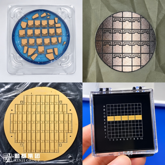
KINJI diamond AMB process product display
This route differs in significance from Sanan's heatsink plates: heatsink plates solve the problem of "attaching a piece of high-thermal-conductivity material to the back of a chip," while AMB substrates solve "heat dissipation and wiring integration within the packaging structure itself." Both belong to "heatsink-grade commercialization," but BNYB's case shows diamond cooling is extending from standalone heatsinks to substrate-level integration—the chip is still not diamond; diamond's role is that of substrate material and heat-spreading channel.
Quantum sensing: mass-production-level engineering cases have emerged
As the core sensitive material for quantum sensing, NV color-center diamond saw landmark engineering deployment in 2026. China Southern Power Grid's ±800 kV UHVDC quantum current sensor has achieved mass production, with a measurement range covering 1 mA to 10 kA and maximum accuracy of 0.06%FS, better than the 0.2-class specification of incumbent fiber-optic transformers; the equipment has operated stably for more than 2,000 hours at an altitude of 2,328 meters in Jianchuan, Yunnan, in an area of seismic intensity 8 and under strong electromagnetic interference. The carbon isotope purity of the core sensitive material, NV color-center diamond, was raised from 99.99% to 99.999%. This is the first case among diamond-related technologies to carry both the "mass production" and "long-term operation in industrial field" labels, but its driver is quantum precision measurement, not power electronics.
Laboratory prototypes: medium- and long-term potential of active power devices
UHVDC transmission, high-voltage grid circuit breakers, high-temperature power conversion for aerospace/aeroengines/oil and gas deep wells, and high-power radar RF power amplifiers are the theoretical target markets for diamond active devices. SBD and hydrogen-terminated MOSFET prototypes have proven "the principle works," but wafer size, defect density, n-type doping and contact processes together determine that these scenarios will more likely land over a decade-plus timescale as "niche applications under extreme conditions" rather than "large-scale replacement of SiC/GaN."
V. Core Bottlenecks: Why Diamond Cannot Replace SiC/GaN in the Short Term
First, the gap between active-grade large-size single crystals and low-cost manufacturing. Heatsink-grade polycrystalline/single-crystal diamond can reach larger sizes, but semiconductor active layers require extremely low defect density and highly controllable doping; usable area and cost are far from the economic threshold of silicon-based production lines. A tiny dislocation can directly cause breakdown of high-voltage devices at field strengths on the order of 10 MV/cm.
Second, the stability and controllability of n-type doping have not passed muster. Without reliable n-type doping, there is no CMOS, no digital logic and no large-scale integration. Phosphorus doping and co-doping research are advancing, but there is still a substantive distance to "repeatable, yield-capable" status.
Third, processing and contact processes are far from mature. Diamond's extreme hardness makes etching, ion implantation and ohmic contacts much more difficult than SiC/GaN; metal–diamond contact resistance is relatively high, directly eroding the theoretical on-resistance advantage.
Fourth, a yield system has yet to be established. SiC and GaN have already walked, or are walking, the industrialization curve of "defect control—yield improvement—cost reduction," while diamond active devices remain at an early stage on this front.
Conclusion
Diamond's material parameters do point to the theoretical ceiling of the "ultimate semiconductor," but ultimate performance does not equal ultimate manufacturability. The real value distribution today is: cooling substrates are already commercial, NV color-center quantum sensing has produced mass-production-level engineering cases, and active power devices remain at the laboratory prototype stage. In the short term, diamond will not rapidly replace SiC/GaN; its realistic role is as a high-end thermal management material in high-power-density scenarios, and as a "next-generation option" being progressively validated in quantum sensing and extreme-condition power electronics. Only after manufacturable-level breakthroughs on the three bottlenecks—n-type doping, active-grade large-size single crystals and contact processes—will the "ultimate semiconductor" have the precondition to move from a theoretical narrative to an industrial one.
trending news
Contact Us