





Sorry, no sales person is available right now to take your call. Pls leave a message and we will reply to you via email as soon as possible.
Diamond Substrate Industry Evolution: From Semiconductor Processing Consumables to Core Chip Thermal Management Materials
2026-08-27
As thermal flux densities in AI high-performance computing chips and third-generation power semiconductor devices continue to rise, traditional copper-based heat dissipation and system-level liquid cooling solutions are struggling to address core pain points such as localized hot spots in transistors and instantaneous heat accumulation. This has triggered a structural revaluation of diamond's role in the semiconductor industry—evolving from its traditional reliance on extreme hardness as a wafer processing consumable, to a core thermal management functional material that leverages its ultra-high thermal conductivity to directly serve chips during their operational phase.
Today, high-quality CVD diamond thin films, sheets, and their composite materials are being progressively integrated into critical locations including chip backside surfaces, GaN device substrates, and package thermal spreading layers. The industry's core logic is clear: diamond does not replace air cooling or liquid cooling; rather, it spreads localized high temperatures and reduces chip junction temperatures at the very point of heat generation, forming a synergistic thermal management system with downstream liquid cooling to address the structural challenge of "sufficient back-end cooling but inadequate front-end heat extraction."
I. Core Material Properties of Diamond: Dual Enablement of Hard-Brittle Machining and Ultra-High Thermal Conductivity
Diamond and graphite are both carbon allotropes, yet their performance differences stem from distinct crystal lattice structures. In diamond, carbon atoms are bonded in a three-dimensional tetrahedral dense lattice, resulting in high structural stability and strong bonding energy. This endows diamond with two critical properties that are rarely found together in the semiconductor industry, both precisely aligned with chip thermal dissipation requirements.
· Extreme Hardness: Its ultra-high hardness enables precision machining of hard-brittle semiconductor materials such as silicon, silicon carbide, and sapphire. Diamond has long served as a core consumable for wafer dicing, thinning, polishing, and scribing, meeting stringent demands for low-damage, high-precision manufacturing.
· Ultra-High Thermal Conductivity: Diamond conducts heat via lattice vibrations (phonons), with lightweight carbon atoms and low bonding losses. High-quality CVD/single-crystal diamond achieves room-temperature thermal conductivity of 1,000–2,200 W/(m·K), with premium products exceeding 2,200 W/(m·K)—approximately 4–5 times that of copper (≈400 W/(m·K)) and over 10 times that of silicon (130–150 W/(m·K)), making it one of the best commercially available thermally conductive materials.
Additionally, high-purity undoped diamond is an ultra-wide-bandgap insulating material (bandgap 5.47 eV), featuring high electrical insulation and low dielectric constant. Its coefficient of thermal expansion (1.0 ppm/K) closely matches that of silicon chips (2.6 ppm/K), allowing close-proximity attachment to heat sources without short-circuit risks, while significantly enhancing package reliability under thermal cycling conditions.
Currently, diamond-based logic chips remain constrained by doping processes, large-area fabrication challenges, and ecosystem immaturity, making large-scale commercialization difficult. High-end thermal dissipation materials, however, represent the most certain and fastest path to industrialization.
Room‑Temperature Thermal Conductivity: Mainstream Semiconductor Materials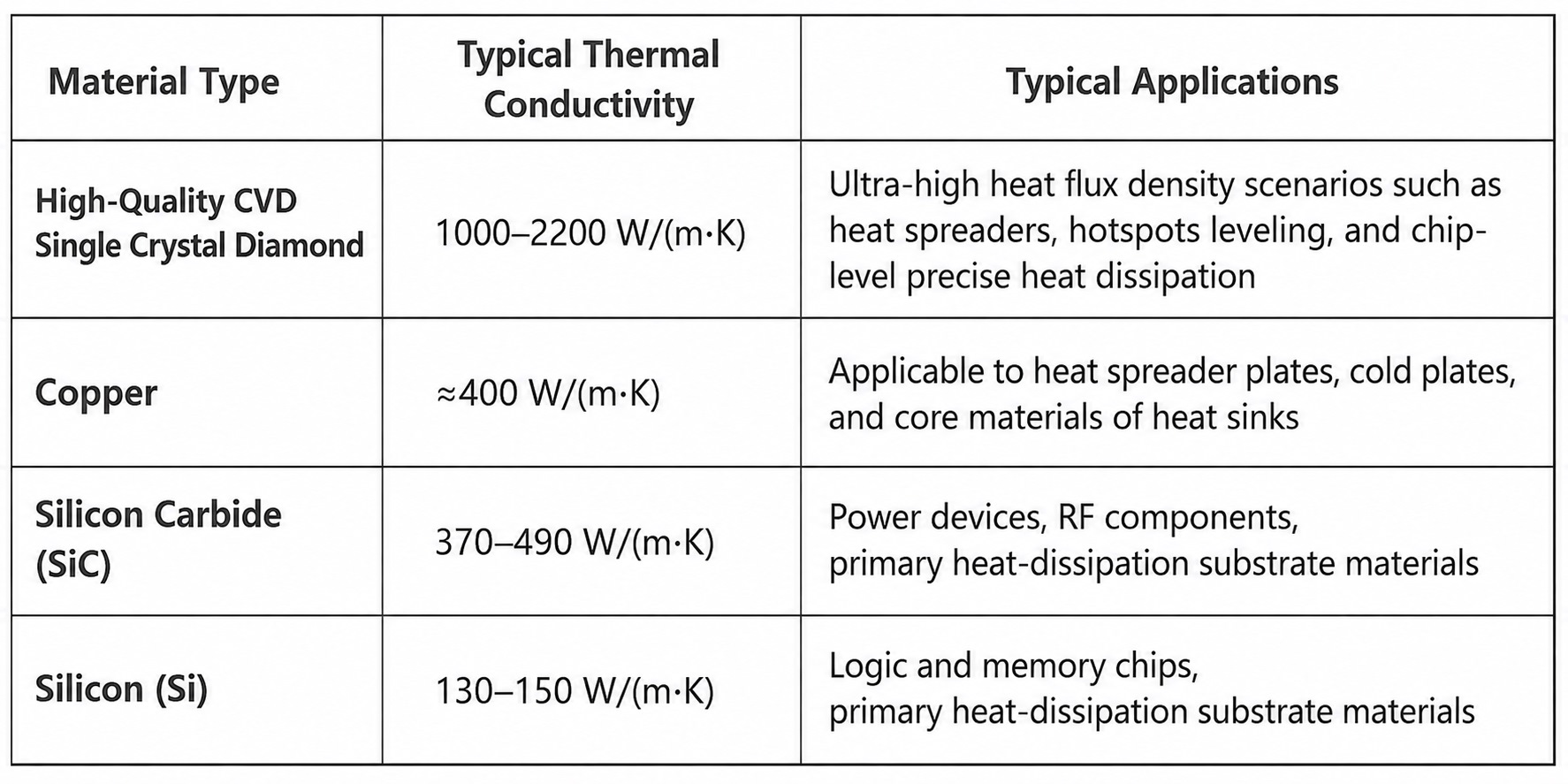
II. Two Major Technical Routes for Synthetic Diamond: CVD Tailored for High-End Thermal Dissipation
Mainstream synthetic diamond production is divided into two primary routes—HPHT and CVD—each with distinct application boundaries, with semiconductor thermal dissipation relying exclusively on the CVD approach:
· HPHT (High Pressure, High Temperature): Produces bulk industrial diamond, primarily single crystals and micro-powders, with high output and low cost. However, purity, uniformity, and defect levels fall short of chip thermal dissipation requirements, making it suitable mainly for consumables such as cutting wires and grinding wheels.
· CVD (Chemical Vapor Deposition): Grows diamond layer by layer from the gas phase, enabling production of high-purity, low-defect, large-area diamond films and thick plates with excellent consistency and stable thermal conductivity. This makes CVD diamond the core raw material for chip heat sinks and device substrate heat dissipation, and a primary area of industry focus.
III. Traditional Applications: Diamond's Role as Semiconductor Consumables
Prior to its adoption in thermal dissipation, diamond long served as a critical precision consumable in semiconductor wafer manufacturing, supporting wafer shaping, finishing, and dicing processes. It participated solely as a consumable tool in the manufacturing phase without being involved in chip operation—characterized by "consumable-on-use, tool-oriented, low-value-add" attributes. Core applications include four categories:
· Ingot Slicing: Diamond wire saws cut silicon and silicon carbide ingots at high speed to produce ultra-thin wafers, widely used in photovoltaics and semiconductor volume production.
· Wafer Backside Grinding: Diamond grinding wheels precisely thin wafer backside surfaces to meet the requirements of advanced packaging, 3D stacking, and power device thinning—directly impacting wafer yield and packaging reliability.
· Wafer Dicing: Ultra-thin diamond dicing blades achieve low chipping and narrow kerf widths for high-speed die separation, ensuring bare die formation yield.
· CMP Pad Conditioning: Diamond conditioning disks restore pad surface topography, resolving pore clogging and roughness degradation issues to stabilize wafer planarization process accuracy.
IV. Industry Transformation: Diamond Enters the Front-End Core Thermal Dissipation Chain
The complete chip thermal dissipation path is: transistor hot spots → silicon/GaN substrate → thermal interface layer → package structure → cold plate/heat sink → coolant/air. Current liquid cooling solutions optimize only back-end heat removal and fail to address localized high heat flux accumulation at transistor sites or the excessively long front-end thermal path, resulting in elevated chip junction temperatures and performance constraints.
Diamond's core value lies in bridging the "last millimeter at the heat source"—rapidly spreading heat laterally and conducting it vertically before thermal diffusion occurs, suppressing hot spot temperature rise at the source. The industry has developed four mature technical routes:
· Standalone CVD Diamond Heat Sink (Mass-Produced): Diamond plates, after metallization and bonding, are placed between the chip and package lid/heat sink to rapidly spread concentrated hot spots and reduce localized heat flux density, suitable for AI and other high-power chip applications.
· Chip Backside Diamond Integration (Advanced Packaging): Diamond films are bonded or deposited onto thinned wafer backside surfaces, shortening the distance between heat source and high-thermal-conductivity material while mitigating silicon layer thermal resistance—ideal for 2.5D/3D advanced stacked packaging.
· GaN-on-Diamond Substrate Replacement (High-End Scenarios): Native silicon carbide substrates are removed from GaN devices and replaced with diamond substrates, achieving zero-distance heat extraction from the source. This approach targets aerospace, military radar, high-end RF, and other high-power, high-junction-temperature-sensitive applications.
· Diamond-Copper Composite Materials (Cost-Effective Mainstream): Diamond micro-powders are incorporated to optimize copper-based material performance, circumventing the processing difficulties and high costs of pure diamond. With stable thermal conductivity of 700–850 W/(m·K), ease of forming, and mass-production compatibility, this represents the fastest-deploying and most widely adopted thermal solution to date.
· Processing Practice Case: Among the above technical routes, precision processing of diamond substrates has remained a critical bottleneck for engineering implementation. Kinji Group, leveraging its advanced diamond substrate processing capabilities, has achieved substantive breakthroughs in CVD diamond heat spreader metallization, laser precision forming, and ultra-thin hole drilling. Its processing techniques meet the stringent requirements of chip backside integration and standalone heat sinks for dimensional tolerances, surface roughness, and metal layer adhesion strength. The company has provided customized diamond substrate samples to multiple packaging manufacturers, effectively reducing interfacial thermal resistance and accelerating the transition of CVD diamond from laboratory samples to production-grade engineering components.
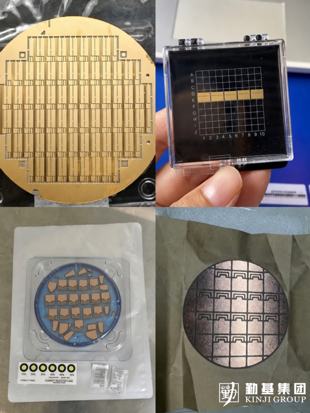
Kinji Group CVD Diamond Substrates
V. Four Core Bottlenecks to Scaled Commercialization
Despite its exceptional theoretical properties, widespread adoption of diamond is not constrained by thermal conductivity figures but rather by engineering, reliability, and cost barriers:
· Interfacial Thermal Resistance as Central Challenge: Bonding interfaces between diamond and silicon, GaN, or metals are prone to voids, non-uniform layer thickness, and poor adhesion, generating high thermal resistance that significantly undermines thermal performance. Low-temperature activated bonding and nano-metal bonding are currently the key process development areas.
· Difficulty in Large-Area High-Uniformity Production: Small-scale laboratory samples with high thermal conductivity are technologically mature, but inch-scale and wafer-scale products must simultaneously achieve uniformity, low defect density, and crack-free integrity—posing extreme challenges in production yield and cost control.
· Processing and Long-Term Reliability Limitations: Diamond's extreme hardness makes precision forming, drilling, and polishing exceptionally difficult. Meanwhile, CTE mismatches with semiconductor materials can lead to delamination, warpage, and cracking under thermal cycling. In this regard, Kinji Group has significantly improved thermal cycling stability of diamond substrates through optimized laser cutting parameters and multi-step annealing processes; its processing solutions have passed reliability validation with select customers, laying the groundwork for subsequent volume deliveries.
· Cost Gradient Constraining Downward Penetration: High-quality CVD diamond remains costly, limiting rapid proliferation into consumer-grade products. Industrialization follows a tiered adoption path: "aerospace/defense → high-end RF/laser → AI servers → high-end consumer electronics."
Key industry maturity indicators include: stable large-area supply capability, controllable low-thermal-resistance interface levels, long-term thermal cycling reliability, and validated repeat customer orders.
VI. Industry Summary and Strategic Positioning
The current thermal dissipation architecture for computing power operates in a layered and collaborative manner: facility air conditioning manages ambient temperatures, liquid cooling manages rack and cold plate temperatures, thermal interface materials manage package contact temperatures, and diamond specifically targets hot spot management at the chip heat source—complementing rather than replacing existing cooling solutions. Even with diamond-based thermal dissipation structures, high-power chips still require downstream liquid cooling, cold plates, and CDU units to complete final heat rejection. Diamond's core value lies in resolving the structural deficiency of "sufficient back-end cooling but severe front-end heat accumulation."
This industry evolution marks a critical value upgrade for synthetic diamond—transitioning from low-end processing consumables reliant on hardness, to high-end semiconductor packaging and thermal management core materials leveraging ultra-high thermal conductivity, electrical insulation, and reliability. Future competitive differentiation in this sector will not be defined by laboratory-record extreme parameters, but by large-area production capacity, low-thermal-resistance process capability, long-term reliability assurance, and scaled delivery execution.
As AI compute chips and third-generation semiconductors continue to gain penetration, CVD diamond thermal dissipation materials are poised to become a standard feature in high-end semiconductor thermal management, opening substantial new growth opportunities across the entire industry value chain.
trending news
Contact Us