





Sorry, no sales person is available right now to take your call. Pls leave a message and we will reply to you via email as soon as possible.
Comprehensive Analysis of PCB Copper Thickness: Parameter Standards, Design Essentials, and Industry Development Trends
2026-07-16
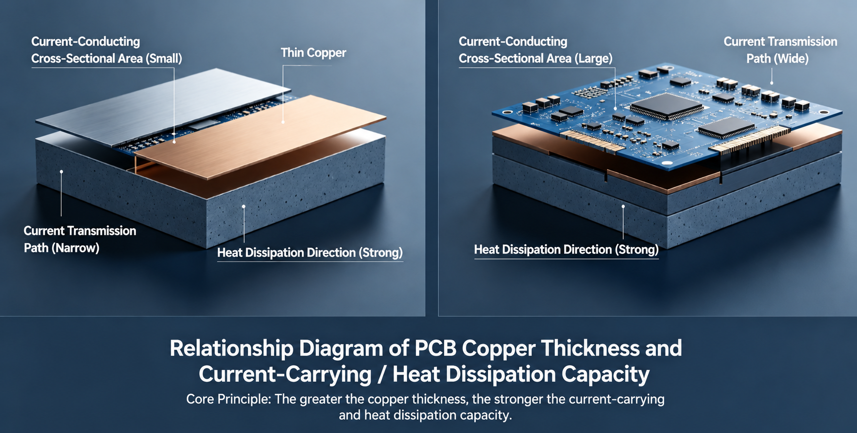
Copper thickness is a core parameter in PCB design and manufacturing, directly determining the circuit board's current-carrying capacity, heat dissipation efficiency, signal integrity, and long-term operational reliability. PCB copper foil can be viewed as the circuit's "conductive and heat-dissipating channel": the greater the copper thickness, the more ample the conductive and heat-dissipating cross-section, leading to a higher current-carrying capacity and better heat dissipation. This effectively prevents circuit overheating and burnout under high-power conditions. Its selection is tailored to products across all fields, including consumer electronics, industrial control, new energy, and aerospace, serving as the foundation for ensuring stable PCB operation. This article, combined with industry practical case studies, systematically analyzes PCB copper thickness parameter standards, design essentials, production inspection specifications, and industry development trends.

I. Copper Thickness Units and Industry General Standards
Precisely mastering the measurement units and specification standards for copper thickness is a core prerequisite for avoiding design and production deviations and matching product scenario requirements. Currently, the global PCB industry has formed unified and common measurement specifications and grade standards.
(I) Commonly Used Measurement Units
The industry-standard unit for measuring PCB copper thickness is the ounce (oz), defined as: the thickness of copper foil formed by uniformly spreading 1 ounce (approximately 28.35g) of pure copper over a surface area of 1 square foot (approximately 0.093 m²) on a copper-clad laminate. The common industry conversion formulas are as follows:
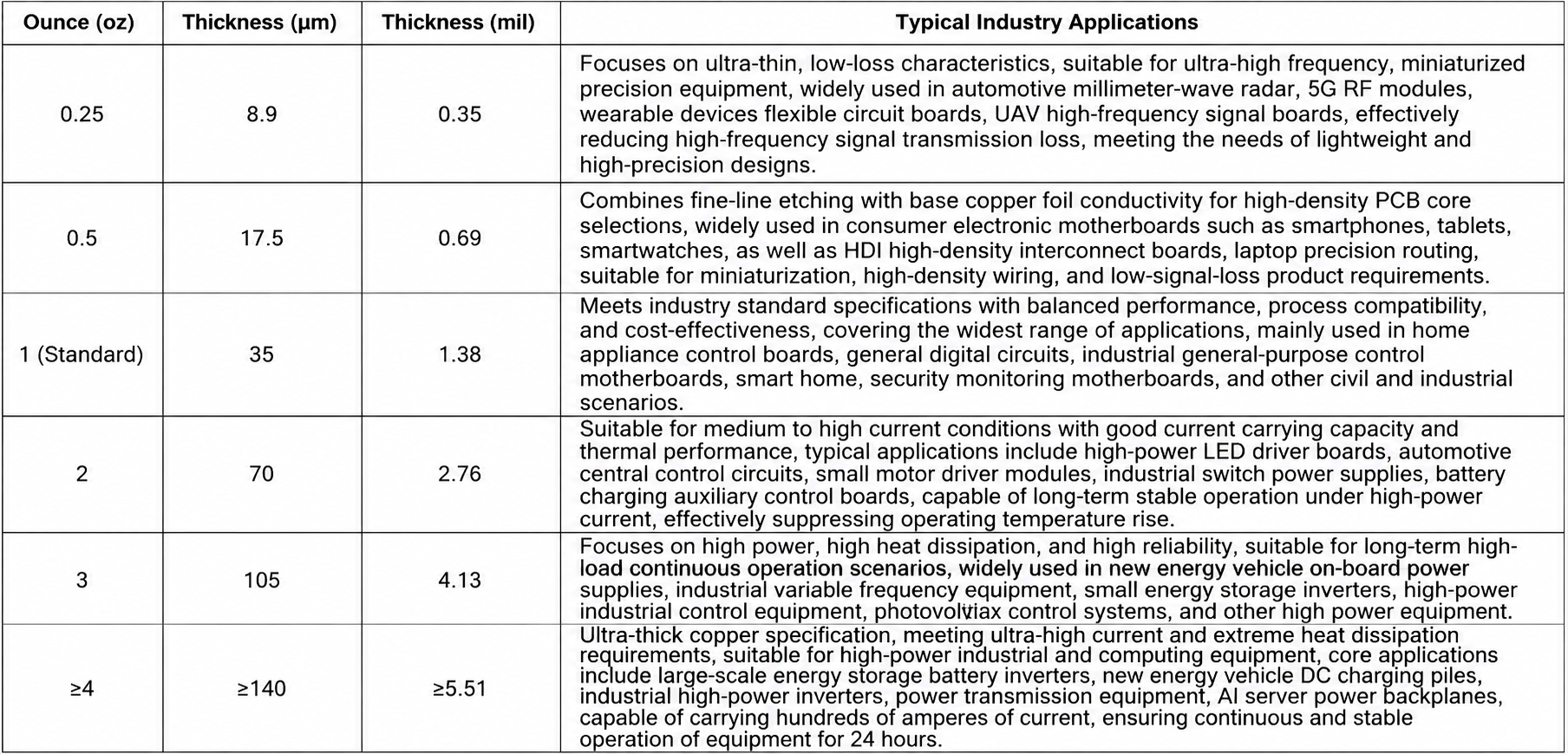
1oz copper foil ≈ 35μm (micrometers) ≈ 1.38mil (thousandths of an inch)
Among these, the ounce is the standard unit for industry selection and marking, the micrometer is commonly used in domestic precision production, and the mil is a common unit in European and American industries. The three can be quickly converted to suit different design and production scenarios.
(II) Mainstream Copper Thickness Specifications and Applicable Scenarios
Different copper thicknesses exhibit significant differences in conductivity, heat dissipation, and mechanical properties, with clearly defined applicable scenarios. The table below summarizes the industry's mainstream copper thickness specifications and corresponding application cases. Parameters and applications are clearly matched, providing a straightforward reference for selection.

(III) Base Copper, Finished Copper Thickness, and IPC International Standards
PCB design and production must strictly distinguish between base copper and finished copper thickness. These are core indicators for process control and parameter design, directly impacting the final product's performance and must not be confused.
· Base Copper: The original thickness of the copper foil on the copper-clad laminate as shipped from the factory. It is a fundamental parameter of the base material, untouched by subsequent manufacturing processes like plating, etching, or surface finishing.
· Finished Copper Thickness: The final copper layer thickness after the PCB has undergone the entire manufacturing process, including drilling, electroless copper deposition, electroplating, etching, and solder mask application. This is the effective thickness for the circuit's actual conductive operation and must be the core basis for engineering design. Industry-standard electroplating processes typically add 20-25μm to the base copper thickness, a standard process increment.
The globally recognized general specification is the IPC-6012 Performance Specification for PCBs. This standard, graded by application reliability, specifies the finished copper thickness, uniformity, and quality requirements for different scenarios. For example, with 1oz base copper, the standard finished copper thickness after plating is 55–60μm. Class 2 is the general consumer grade, suitable for home appliances and standard consumer electronics. Class 3 is the high-reliability industrial grade, with stricter requirements for minimum copper thickness, uniformity, and adhesion. It is specifically for high-precision, high-reliability scenarios like automotive, aerospace, and high-end industrial control, effectively preventing circuit failure under complex operating conditions.
II. Core Design Considerations for Copper Thickness Selection
Choosing the right copper thickness is not simply a matter of "the thicker, the better." It requires a comprehensive trade-off involving product operating conditions, electrical performance, usage environment, and production costs. Current-carrying capacity and temperature rise control, signal integrity, heat dissipation performance, and mechanical reliability are the four core design considerations.
(I) Current-Carrying Capacity and Temperature Rise Control
Current flowing through PCB traces generates Joule heat. According to the IPC-2221 generic standard for PCB design, copper thickness and trace width together determine the current-carrying capacity limit and temperature rise. The greater the copper thickness, the larger the conductive cross-section, the lower the trace resistance, and the lower the heat generated for the same current, resulting in higher current-carrying capacity.
Industry test data: At room temperature with a 10°C temperature rise, a 1mm wide trace with 1oz copper can stably carry 2A of current. Under the same conditions, a 2oz copper trace can carry 4A, doubling the current-carrying performance.
Industry application case: Ordinary home power supply boards typically use the standard 1oz copper thickness to meet conventional current-carrying and temperature rise requirements. However, output circuits in new energy vehicle charging piles can experience instantaneous currents of up to hundreds of amperes. The industry commonly uses 3oz or thicker copper combined with widened trace designs to strictly control operating temperature rise, preventing circuit faults caused by long-term high-temperature aging and ensuring continuous and stable operation of the charging equipment.
(II) Signal Integrity in High-Frequency Scenarios
In high-frequency, high-speed scenarios like 5G and millimeter-wave, the skin effect must be carefully managed: during high-frequency signal transmission, current flows only along the very thin surface layer of the copper foil, while the inner copper carries no current. Blindly thickening the copper foil not only fails to improve performance but can increase dielectric loss, leading to signal attenuation, impedance mismatch, signal crosstalk, and other problems that compromise signal integrity.
Industry best practice optimization solution: For high-frequency high-speed circuits, prioritize using 0.25oz–0.5oz ultra-thin, low-profile, smooth copper foil to minimize signal transmission loss.
Industry application case: High-frequency PCBs in equipment like Huawei and ZTE's 5G base station RF boards and automotive millimeter-wave radar all standardly use 0.5oz ultra-thin, low-roughness copper materials. This significantly reduces insertion loss for millimeter-wave signals, effectively ensuring the accuracy and stability of high-frequency signal transmission.
(III) Heat Dissipation Performance Optimization
Copper has excellent thermal conductivity and is the PCB's primary heat-dissipating medium. Thickening the copper foil increases the thermal conduction cross-section, creating an efficient built-in heat dissipation channel. This quickly conducts heat away from power chips, MOS tubes, power modules, and other components, preventing localized hot spots. This is crucial for stable operation in high-power, high-density PCBs.
Industry application case: In high-heat-dissipation equipment like industrial high-power LED driver boards and energy storage inverters, PCBs commonly use 2–3oz thick copper optimization. This allows for quick conduction of heat from power components without the need for large external heatsinks, simplifying the equipment structure while significantly improving overall heat dissipation efficiency and long-term operational stability.
(IV) Mechanical Strength and Long-Term Reliability
PCBs are frequently subjected to complex conditions like temperature cycling and vibration shock. Copper thickness directly determines the circuit's mechanical strength and fatigue resistance. Sufficient copper thickness helps buffer the internal thermal expansion and contraction stresses between the copper layer and the base material, preventing issues like plated through-hole cracking, trace lifting, and solder joint failure. It also enhances the trace's tensile and tear strength, reducing the risk of trace fracture under vibration.
Industry application case: In high-reliability scenarios like automotive electronics and aerospace, control circuit boards are mandated to use a minimum finished copper thickness of ≥1oz. High-power automotive circuits are further upgraded to 2oz thick copper designs to withstand wide temperature cycling (-40°C to 125°C) and high-frequency vibration shock, effectively preventing trace cracking and lifting, thus ensuring long-term, trouble-free operation of high-end equipment.

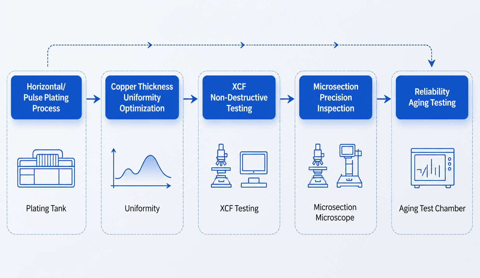
PCB Copper Thickness Production and Inspection Process Flowchart
III. Production Manufacturing, Inspection Standards, and Industry Development Trends
Controlling copper thickness uniformity and precision is a core process challenge in PCB mass production, directly determining product yield and reliability. Driven by upgrades in the new energy, AI computing power, and high-end industrial control sectors, PCB copper thickness processing and inspection technologies are continuously evolving. The industry is progressively advancing towards high precision, intelligence, and high reliability.
(I) Manufacturing Process Challenges and Optimization Solutions
Traditional vertical electroplating processes struggle with products featuring high-aspect-ratio deep holes, thick copper, or fine-pitch circuits. They often result in "dog-bone" defects, where the copper is thicker at the board edges and thinner in the center and within holes. This leads to uneven current distribution, localized overheating, and eventual failure—a primary pain point in mass production.
Currently, leading industry manufacturers commonly employ advanced processes like horizontal continuous plating, pulse plating, and uniform panel plating. By dynamically adjusting current density and solution flow rate, they significantly improve copper layer uniformity across the entire board and within holes, completely solving issues of uneven plating and trace deformation in thick copper PCBs. This enables stable mass production of 4oz and even ultra-thick copper PCBs.
(II) Inspection Methods and Quality Control System
The industry has established a full-dimensional copper thickness quality control system based on a "rapid screening + precise arbitration + reliability verification" approach, strictly adhering to IPC standards to ensure product compliance and stable performance:
1. Rapid Batch Screening: Utilizes X-Ray Fluorescence (XRF) thickness gauges for non-destructive, non-contact testing, suitable for 100% batch inspection to quickly determine if copper thickness meets specifications.
2. Arbitration-Level Precision Inspection: Employs the micro-sectioning analysis method. By cutting, mounting, polishing, and examining cross-sections under a high-power microscope, it precisely measures copper layer thickness and adhesion. This is the ultimate standard for compliance verification in the industry.
3. Reliability Verification: Involves tests such as thermal cycling, thermal shock, and high-temperature aging to simulate extreme operating conditions. This verifies the copper layer's resistance to fatigue and cracking, ensuring the product's long-term stability.
(III) Core Industry Development Trends
Upgrades in downstream industries are driving the evolution of PCB copper thickness technology. The industry has moved beyond simple selection of thick or thin copper, advancing towards precision, differentiation, high reliability, and intelligence. The core trends are:
1. Localized Thick Copper Composite Process Becoming Mainstream:
Traditional whole-board thick copper processes are costly and cannot achieve fine-pitch etching, presenting significant limitations. The current industry trend favors localized thick copper composite technology. This involves thickening the copper layer in high-current power supply areas and power device regions while retaining standard thin copper in signal areas. This approach balances high current-carrying capacity, high-density routing, and cost-effectiveness, and has been widely adopted in products like new energy control boards and AI server power boards.
2. High-Power Sector Driving Surge in Demand for Ultra-Thick Copper PCBs:
The rapid growth of high-power industries like AI servers, new energy vehicles, energy storage, and photovoltaic/wind power is driving continuous increases in PCB power density. This has led to explosive demand for 4oz and above ultra-thick copper PCBs. For instance, large-scale energy storage power stations commonly use 4–6oz ultra-thick copper designs for their converter PCBs to withstand huge continuous currents and operate reliably under 24/7 high-power conditions.
3. Intelligent Upgrades in Production Manufacturing:
Traditional manual process adjustments suffer from large deviations and poor consistency. The industry is now actively promoting intelligent manufacturing upgrades. Leveraging AI algorithms and machine vision systems, manufacturers can monitor electroplating parameters and copper layer uniformity in real-time, dynamically correcting process deviations. This significantly improves copper thickness precision and product yield, enabling stable mass production of high-precision thin copper and ultra-thick copper PCBs.
4. Application Boundaries of High-Reliability Thick Copper PCBs Continue to Broaden:
Leveraging their superior heat dissipation and reliability, thick copper PCBs are gradually expanding into high-end fields such as aerospace, high-end medical equipment, rail transit, and precision military applications. Meanwhile, ultra-thin, low-loss copper foils continue to penetrate the 5G communication and millimeter-wave precision equipment markets. This has created a refined selection pattern where "thin copper for precision scenarios, thick copper for high-power scenarios," with application boundaries constantly expanding.
trending news
Contact Us